


1. Introduction
For the past century, energy consumption has explosively increased with the exponential development of industries and technology. The rapid increase in energy consumption has caused severe environmental pollution and unpredictable climatic changes. To overcome these issues, renewable energy has been explored. Precisely, hydrogen energy has been considered the most promising alternative energy owing to its high energy density and clean and abundant resources. Nevertheless, the use of hydrogen energy has not been expanded owing to insufficient hydrogen storage technology. Conventionally, the storage of hydrogen is accomplished either through compression at a high pressure or liquefaction at 20 K [1, 2]. However, these approaches possess inherent problems with boiling-off, explosion probability, and cost-effectiveness [3].
These drawbacks have directed significant research attention toward a novel hydrogen storage method. Among the various approaches explored, a solid-state hydrogen storage approach using advanced materials such as metal hydride, metal oxides, and porous carbon materials has been considered promising [4–7]. When metal oxides are employed, the hydrogen can be incorporated into the lattice, thereby affecting its electrical properties. Moreover, the rutile phase of vanadium dioxide (VO2) can be doped with hydrogen, which then reversibly diffuses into the lattice [8]. Using this phenomenon, Yoon et al. reported that hydrogen molecules are reversibly adsorbed and desorbed on the lattice of a VO2 thin film. During this process, the formation of interstitial and substitutional defects is expected to decrease, enhancing the storage capacity [8].
In this regard, the influence of hydrogen adsorption on the lattice of a VO2-bulk or powder-type structure still requires further investigation. Investigating the properties of VO2 nanostructure due to the hydrogen sorption on the lattice would be interesting to understand because anodically formed metal oxide nanostructures exhibit several advantages such as high surface area [9–11] and tunable pore diameter or oxide thickness [12–15]. Herein, anodic VO2 nanotubes were formed using [BF4]−-based electrolyte. Subsequently, the textural and hydrogen sorption properties were characterized using Scanning Electron Microscope (SEM), Energy Dispersive X-ray Spectroscopy (EDX), X-ray diffraction (XRD), Brunauer-Emmett-Teller (BET) surface area analysis and volumetric gas uptake analyzer.
2. Experimental
2.1 Formation of the anodized VO2 sample
Vanadium foil (99% purity, 1.5 cm × 1.5 cm) was degreased through ultrasonication in acetone, ethanol, and deionized water consecutively for 10 min. Afterward, the foil was dried using streamed high-purity nitrogen (N2) gas. For the anodization process, a two-electrode system was used comprising the vanadium foil in contact with a 1 cm diameter O-ring as a working electrode and a platinum gauze as a counter electrode. The anodization electrolyte is a mixture of 0.1 M hydrofluoric acid (Sigma Aldrich, HF, 48 wt%) and 20 mM sodium tetrafluoroborate (Sigma Aldrich, NaBF4, 98%) in ethylene glycol (Junsei, 99.5%) solvent. The anodization was conducted using a source meter (Keithley, model 2400) for an hour. During the anodization process, the temperature was maintained at 280 K. After anodization, the sample was immersed in high-purity ethanol to remove electrolyte residue. Subsequently, the anodized vanadium oxide sample was annealed in an Ar-saturated atmosphere at 673 K for 3 h with a heating rate of 3 K/min. Flow rate of Ar gas was 500 sccm, which was controlled using a mass-flow controller.
2.2 Characterization of the anodized VO2 sample
The crystal structure of the anodized VO2 sample was characterized using XRD (X-ray diffractometer (Malvern Panalytical, X’Pert Pro MRD)). Also, the microstructure of the sample was analyzed using a field-emission scanning electron microscope (FESEM, JEOL, JSM-6701F).
2.3 N2 Brunauer-Emmett-Teller (BET) and H2 sorption measurement
To measure BET and H2 sorption measurement VO2 nanotubes were stripped off from metal substrate. The mass of measured VO2 nanotubes was 68.77 mg. Specific surface area (SSA) measurements at 77 K were conducted using an ASAP2020 device with N2 gas. The sample was degassed in vacuum at 400 K for 12 h to remove all adsorbed gas molecules. The SSA was obtained through the multipoint Brunauer-Emmett-Teller (BET) method using a typical relative pressure (P/P0) range of 0.05–0.3. An automated Sievert-type volumetric gas sorption apparatus (PCTpro-E&E) with a micro-doser was used to perform the hydrogen adsorption experiment. Before the gas adsorption measurement, the sample was degassed at 373 K for 6 h under vacuum. Hydrogen isotherms were measured in the gas pressure range of 0–25 bar at 298 and 373 K.
3. Results and Discussion
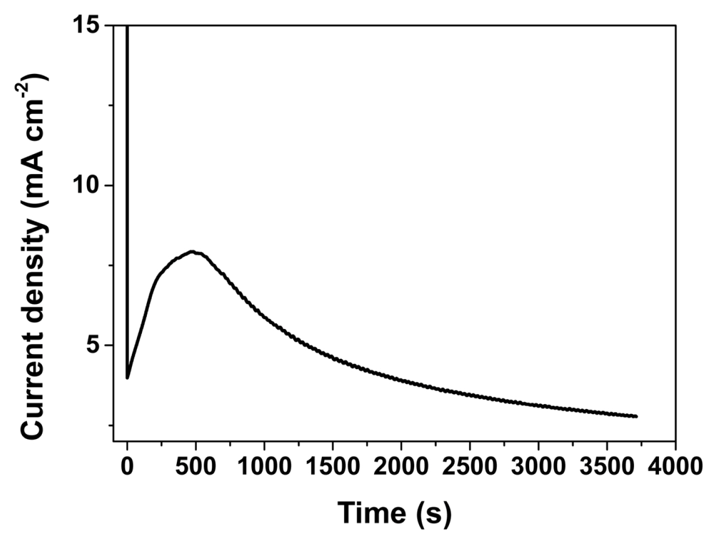
Fig. 1 shows the current density transient during anodization of the vanadium sample performed in 0.1 M HF/20 mM NaBF4/ethylene glycol at 50 V for an hour. The current density transient shows the typical current density behavior during the anodization of a metal sample to form porous or nano-tube structures as described in reference [9,16,17]. At the onset of the anodization, a compact metal oxide layer was formed by O2− or OH− with a high electric field (equation 1). The formed oxide layer dissolves by reacting with the fluoride ion in the electrolyte (equation 2). The anodic metal oxide nanostructure can be formed at the equilibrium state between the formation and dissolution reaction of the oxide [equation. 1 and 2].
where, M and z represent the metal and mean number of electrons engaged in the reaction. Moreover, the drastic increment of the current density to a maximum value of to 7.93 mA/cm2 after approximately 500 s results from the resistance to heat at the early stage of the anodization (Fig. 1) [18]. By maintaining the anodization temperature at 300 K, the dissolution rate could be suppressed, leading to the equilibrium state.
As a result of the anodization of the vanadium metal in a fluoride ion-containing electrolyte, the chemical composition of the anodic vanadium oxide layers would be a mixture of vanadium oxide and vanadium-oxy-fluoride (VOx-Fy) as described in previous studies [19,20]. VOx-Fy easily dissolves in a small amount of water or humidity, even in the atmosphere [20], hence, the as-formed vanadium oxide layer could be detached from the metal substrate or collapse with the amorphous phase. To enhance chemical stability and crystallization, additional heat treatment is required.
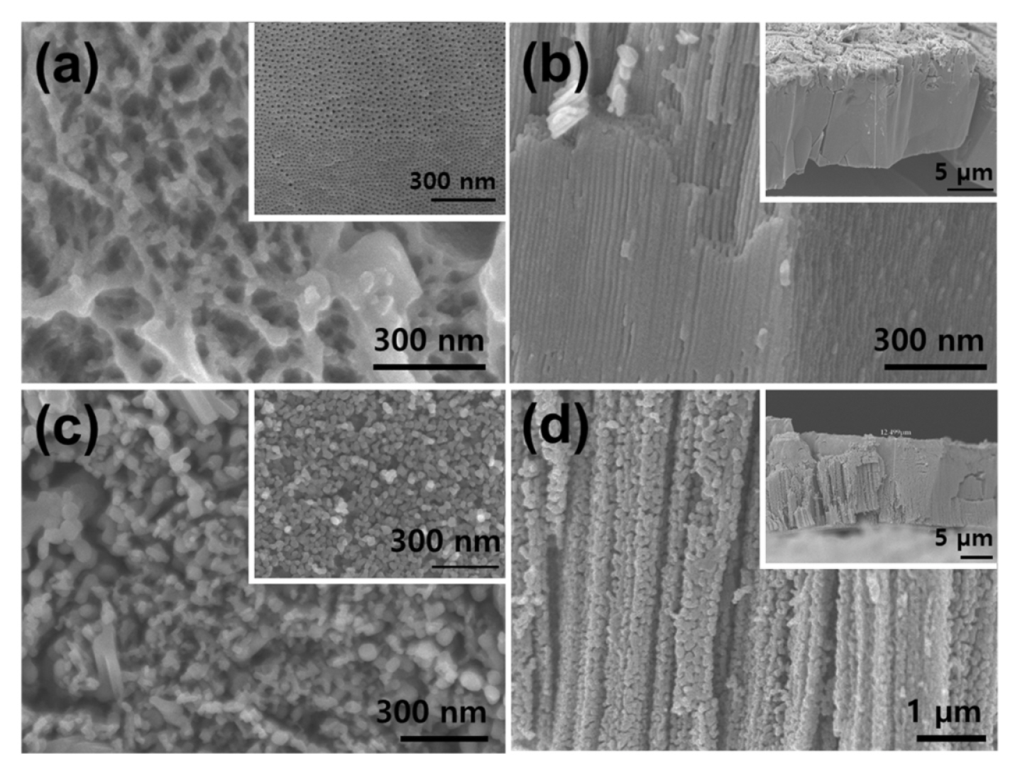
Fig. 2 shows the top-surface and cross-sectional SEM images of anodically formed vanadium oxide layers. The surface morphology of anodic vanadium oxide shows disordered wire-like structures on the surface of the metal sample as shown in Fig. 2(a). The disordered top morphology is a result of the intensive etching reaction by high current flow and heat generation during anodization [21, 22]. Nevertheless, highly ordered nanoporous structures under the wire-like surface of the anodic vanadium oxide were observed as shown in Fig. 2(a) inset. The cross-sectional SEM image in Fig. 2(b), shows that the anodic vanadium oxide layer contains vertically aligned nanotubular structures. From investigation, the thickness and outer diameter of the vanadium oxide nanotubes were approximately 12 μm and 10 nm respectively. To convert the as-formed vanadium oxide nanotubes to VO2 nanotubes, precisely, additional annealing processes were performed. The annealing was carried out 673 K for 3 h in an Ar-saturated atmosphere. The Ar atmosphere allows the conversion of amorphous vanadium oxide to crystalline VO2 structure. When annealed in O2 or atmospheric air, the as-formed vanadium oxides were converted to crystallized V2O5 phase [18–20,23–25].
Fig. 2(c) and (d) show the fully converted VO2 nanotube structures from amorphous vanadium oxides or VOx-Fy. The top-surface morphology in Fig. 2(c) shows the remaining disordered structures and wire-like structures, which are somewhat agglomerated. The cross-sectional view in Fig. 2(d) indicates that the thickness of the nanotubes was about 12 μm. As expected, the nanotube structures were agglomerated, which led to small granule-like structures. Nevertheless, the tubular scaffold of structures remained.
Fig. 3(a) shows the chemical compositions of the VO2 nanotubes which were obtained using EDX. From the investigation, the chemical compositions of the anodic VO2 nanotubes comprise only vanadium and oxygen species. Hence, it is clear that the VOx-Fy was fully converted to oxide structures by the annealing process. Moreover, Fig. 3(b) illustrates the XRD patterns of the annealed vanadium oxide structures. XRD angle (2θ) of 25.22° and 49.41° corresponds to the (110) and (312) planes indicating monoclinic VO2 (JCPDS #00-031-1438). Additionally, the (110), (101), (111), (220), (002) and (112) planes exist at 27.68°, 37.01°, 42.05°, 55.41°, 65.10°, and 72.21°, respectively, as tetragonal VO2 (JCPDS #01-079-1655). The peaks clearly indicate that the annealed anodic vanadium oxide structures are tetragonal VO2 structures.
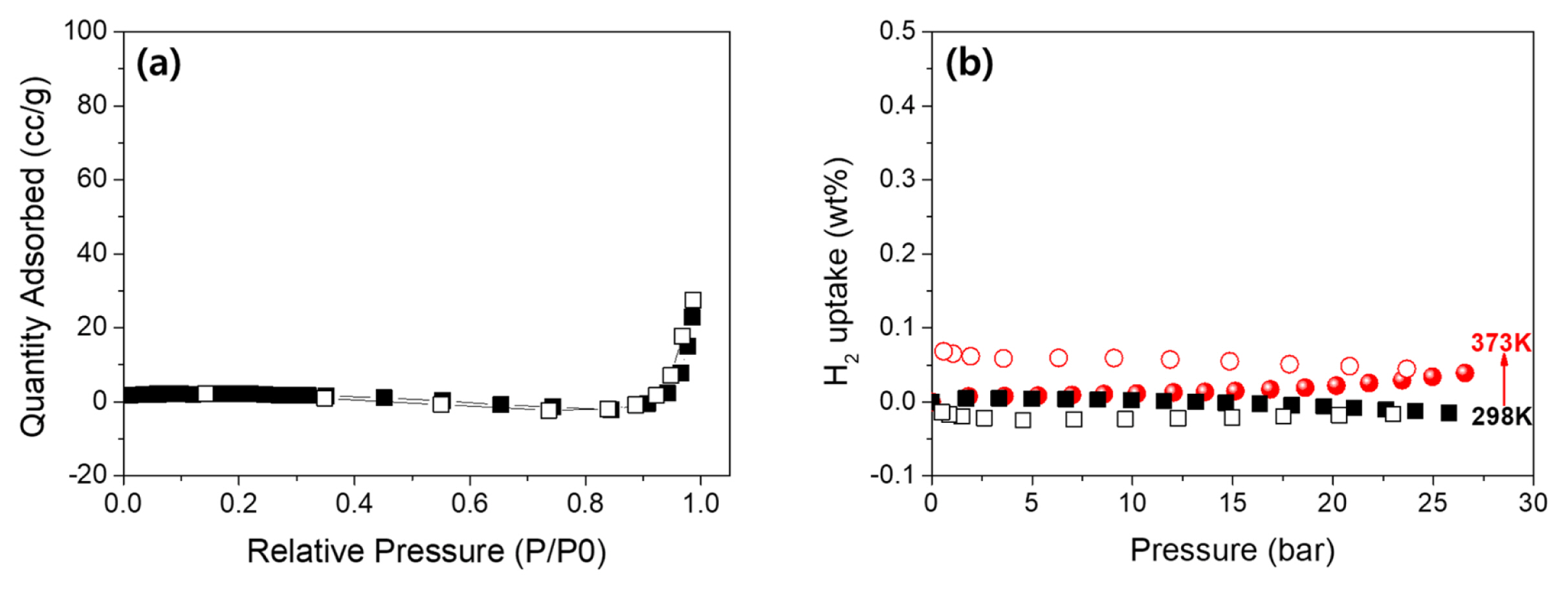
The nitrogen isotherm exhibits an SSA of 5.2 m2/g and a total pore volume (TPV) of 0.035 cm3/g (Fig. 4(a)). Such low SSA and TPV imply that hydrogen sorption will take place in the bulk phase rather than on the surface. To evaluate hydrogen adsorption performances, the hydrogen isotherms of VO2 were measured under various temperatures (298 and 373 K) and from 0 to 25 bar (Fig. 4(b)). At room temperature, hydrogen was hardly adsorbed in the VO2, which may be due to the low thermal energy making it impossible to overcome the activation barrier of bulk diffusion. Conversely, due to the higher thermal energy, the uptake for hydrogen at 373 K and 25 bar increased to 0.04 wt. % with a hysteresis. This also implies that the reversible lattice sorption does not affect the bulk nanostructured VO2 in contrast with that reported for thin films.
4. Conclusions
Herein we investigated the electrochemical formation of VO2 nanotubes and their feasibility for H2 storage. VO2 nanotubes were formed by the anodization of vanadium metal in 0.1 M HF/20 mM NaBF4/ EG. The thickness and diameter of the VO2 nanotubes were about 12 μm and 10 nm, respectively. The low surface area of 5.2 m2/g implies that hydrogen sorption occurred mostly in the bulk phase of the VO2 nanotubes rather than on the surface. Although a strong hysteresis exists, however the hydrogen uptake at 373 K and 25 bar reached 0.04 wt.%. Finally, the sorption mechanism of the VO2 nanotubes does not follow the reversible lattice sorption behavior of VO2 thin films, but rather bulk diffusion with hysteresis.