



1. Introduction
Since the first report of a TiO2 photocatalyst under UV irradiation in 1972 [1], solar-driven hydrogen production has been widely investigated to achieve a clean, renewable, and economical energy source to replace fossil fuels. To achieve high solar-to-hydrogen (STH) conversion efficiency, many strict requirements must be satisfied for each component in the cell, including the photoelectrode materials, electrolyte, device configuration, and connection to the external circuit. Among these requirements, photoelectrode materials have been regarded as crucial components for achieving highly efficient photoelectrochemical (PEC) cells. Accordingly, preparation methods and architectures have been intensively surveyed with the aim of producing ideal-working PEC cells or optimum STH efficiency to realize large-scale solar hydrogen production. In general, photoelectrodes in PEC cells should offer a thermodynamic potential of at least 1.23 V for overall water splitting under solar illumination conditions and an overpotential of 0.2–0.3 V in each photoelectrode should be considered. Therefore, a photoelectrode with an electronic band gap (Eg) of at least 2.0 eV has been suggested, with a close correlation to the optical coefficient. In addition, to achieve a stand-alone PEC cell under no bias, the conduction and valence band edge of the photoelectrode material should be more negative and positive than the H+/H2 and H2O/O2 potentials, respectively, partially enabling to the improvements by the configuration of a tandem cell. Furthermore, material durability in the electrolyte against photo-corrosion during PEC working conditions, good interfacial kinetics, and long diffusion length are necessary for highly-efficient PEC cells [2,3].
Recently, III-nitride nanostructures have been identified and reported as promising candidate materials in solar-driven water splitting due to their high thermal stability, excellent chemical stability, and tunable bandgap by the addition of Al or In sources [4–6]. The Eg of GaN is appropriate for water splitting because it straddles the reduction and oxidation potential of water. There have been intense research efforts to improve the PEC performance by developing low dimensional GaN nanostructures (such as nanorods, nanowires, and nanopores), which can increase the light absorption capacity and the charge collection efficiency. However, GaN nanowires revealed sufficient surface states which result in surface Fermi level pinning to act on the nonradiative recombination center [7]. In addition, GaN undergoes surface oxidation under PEC conditions (creating a thin amorphous GaOx layer) and suffers from indigent alkaline instability, hindering the improvement of PEC performance. Furthermore, most of the conventional nanorods and wires were developed using complicated manufacturing processes, resulting in high development costs. Also, the radiation-induced damage and the exposed surface states can result in reduced device performance [8,9].
To overcome the aforementioned difficulties, the great care should be taken to enhance the surface properties of GaN. One emerging method to enhance PEC performance is surface treatment (or surface engineering) of the photoelectrode. This inorganic surface treatment can provide favorable charge transfer events under reduced surface defect density, leading to shift Ferimi level upward and enhancing the durability of PEC cells. Herein, to exclude the surface nanotexturing effect and increased surface states, the bulk GaN wafer is adapted to investigate the surface effects of NH3 treatment. The NH3 annealing condition is optimized and the surface/interfacial effects on PEC activity are discussed in detail compared to an untreated GaN wafer.
2. Experimental
2.1 GaN Growth and NH3 Post-Treatment
The un-doped n-type GaN (developed on a sapphire substrate) was grown by metal–organic chemical vapor deposition (MOCVD). Trimethylgallium (TMGa, 195 μmol·min−1) and NH3 (99.9999%, 424 mmol·min−1) were used as precursors for the gallium and nitrogen, respectively. Then, the reactor temperature was increased to 1190°C and the growth time was fixed at 6400 s to obtain a GaN film of ~3 μm thickness with a carrier concentration of 2 × 1018 cm−3. During growth, the reactor pressure was maintained at 100 torr, and H2 was used as the main carrier gas. The pristine GaN was treated by annealing in a tube furnace at 900°C for 10 min under NH3 (99.999% purity) atmosphere.
2.2 Characterization
A high-resolution X-Ray diffraction (HR-XRD, PANalytical, X’Pert PRO) instrument operating at 40 kV and 30 mA was employed to reveal detailed information on the crystalline properties of the GaN films. Moreover, field emission-scanning electron microscopy (FE-SEM) images were recorded on an S4800 (Hitachi Inc. instrument) at a 20 kV acceleration voltage. The UV-vis spectra were collected using PerkinElmer UV-vis Lambda 365 spectrometry, recorded in a wavelength range of 250–400 nm. The chemical composition and states of each element were analyzed by X-ray photoelectron spectroscopy (XPS, NEXSA, Thermo Fisher) with monochromatic Mg Kα (hv = 1253.6 eV) radiation under an ultrahigh vacuum (<10−7 torr).
Linear sweep voltammetry (LSV) in chopping mode (on/off interval time = 2 s) was conducted at a scan rate of 20 mV·s−1 from −0.5 to +1.5 VRHE during the potential sweep in a standard three-electrode configuration: working, platinum counter, and homemade saturated Ag/AgCl electrodes (0.11 V vs. normal hydrogen electrode). This potential was converted to RHE (= NHE at pH = 0), using the following equation (1):
An aqueous electrolyte containing 1 M NaOH (pH = 13.5) was used for the PEC test, and a Newport Oriel Xenon 150 W solar light simulator (100 mW·cm−2, AM 1.5 G) was used as the light source. The calibration of 1 sun illumination complied with NREL-certified Si photodiodes. The incident photon-to-current converSoon Hyung Kang et al. / J. Electrochem. Sci. Technol., Epub ahead of print 3 sion Efficiency (IPCE) was measured as a function of wavelength from 340 to 400 nm at an applied potential of 1.23 VRHE using an IPCE system designed for PEC water splitting. In addition, electrochemical impedance spectroscopy (EIS) of all the samples was conducted to estimate the cell resistance of each component. The working condition was measured using a standard potentiostat (Autolab/PGSTAT, 128N) equipped with an impedance-spectra analyzer (Nova). The measured frequency range was from 0.1 Hz to 10 kHz at an amplitude of ±10 mV. Moreover, to measure the flat-band potentials (VFB) and charge carrier densities of the films, Mott-Schottky plots (Autolab /PGSTAT, 128N) at frequencies of 1 kHz were taken using a standard potentiostat equipped with an impedance spectra analyzer (Nova) using the same electrochemical configuration and electrolyte under dark conditions.
The H2/O2 gas was detected using a gas chromatograph–mass spectrometer (YL Instrument 6500 GC System) equipped with a TCD/FID detector under a flow of Ar (99.999%) carrier gas. The amount of total charge (Q) passing through the photoelectrode was measured by an amperometric curve at a constant potential of 1.23 VRHE with respect to time. The amount of gas evolution was determined by sampling 250 μL of the evolved gas from the headspace of the compartment using a gas-tight syringe every 15 min. The Faradaic Efficiency (FE) was calculated by dividing the amount of gas detected by the theoretical amount of gas calculated based on the total charge passed using the following equation (2) [10]:
where z is the evolved O2 (mol) gas, n is the electron involved in the reaction (n=4), F is the faradic constant (96485 C·mol−1), and Q is the charge passing through the working electrode.
3. Results and Discussion
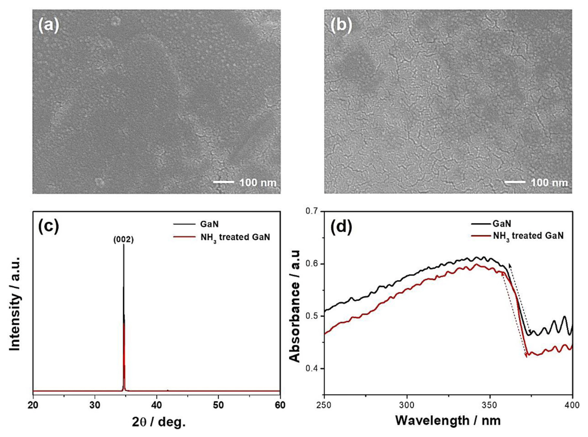
Fig. 1 displays the FE-SEM images, XRD patterns, and UV-VIS spectra of the GaN and NH3-treated GaN films. After NH3 treatment, no remarkable change in the surface morphologies was revealed (Fig. 1(a,b)), although a small increase in the number of cracks on the top surface area was observed. The GaN film exhibited a highly crystalline wurtzite structure with the (002) plane at 34.6°, and the NH3-treated GaN film exhibited a similar crystal structure and reduced intensity. This was probably caused by the appearance of some cracks in the surface region as well as the stressed GaN film under the excessive N element. Other diffraction peaks related to GaOx were not revealed anywhere, providing strong evidence that the GaN was grown by only a single crystalline phase [11,12]. In addition, there was no peak shift closely correlated with the vacancies of Ga or N ions. The optical properties of both films were surveyed using a UV-Vis spectrophotometer, as displayed in Fig. 1(d). Overall, these spectra indicated that both films displayed significant light absorption from ~375 nm and slightly enhanced light absorption was achieved in NH3-treated GaN film under a similar onset wavelength for meaningful light absorption. More detail, the optical bandgap from Tauc plots were calculated to show 3.09 eV and 3.17 eV at the GaN and NH3 treated GaN films (not shown here), revealing the no significant optical change after NH3 treatment.
X-ray Photoelectron Spectroscopy (XPS) was adopted to investigate the surface composition and chemical states of the Ga and N species in all the films, as summarized in Fig. 2(a–d). From the widescan XPS spectrum of GaN films (Fig. 2(a)), Ga and N species were present in the film. Moreover, for the core-level Ga3d spectra, a peak at a binding energy (BE) of 19.61 eV was observed in the GaN film, while the NH3-treated GaN film exhibited a peak at a BE of 19.74 eV, positioned at the high BE site of approximately 0.13 eV [13]. To examine the chemical states of the N1s element, the core-level N1s peaks of each film were compared, as shown in Fig. 7(c). The peaks at a BE of 396.71 eV originated from the GaN film, while a shift (~1.7 eV) toward the high BE site was observed in the NH3-treated GaN film. For the core-level O1s spectra, the GaN still possessed a peak at a BE of 531 eV, implying the presence of oxygen elements, while the NH3-treated GaN film exhibited a similar peak at a BE of 531.4 eV, revealing a shift toward the high BE site. All elements exhibited a peak shift toward the high BE site in the NH3-treated GaN film, which could be explained by the formation of N-Ga-O bonding in the circumstance of Ga-O bonding, partially shifting the electron density from the O elements to the N elements. Therefore, it could be inferred that a small amount of the GaOx phase was formed on the surface region of the GaN film and the GaOx phase was transformed to the GaOxN1-x phase under excessive NH3 treatment.
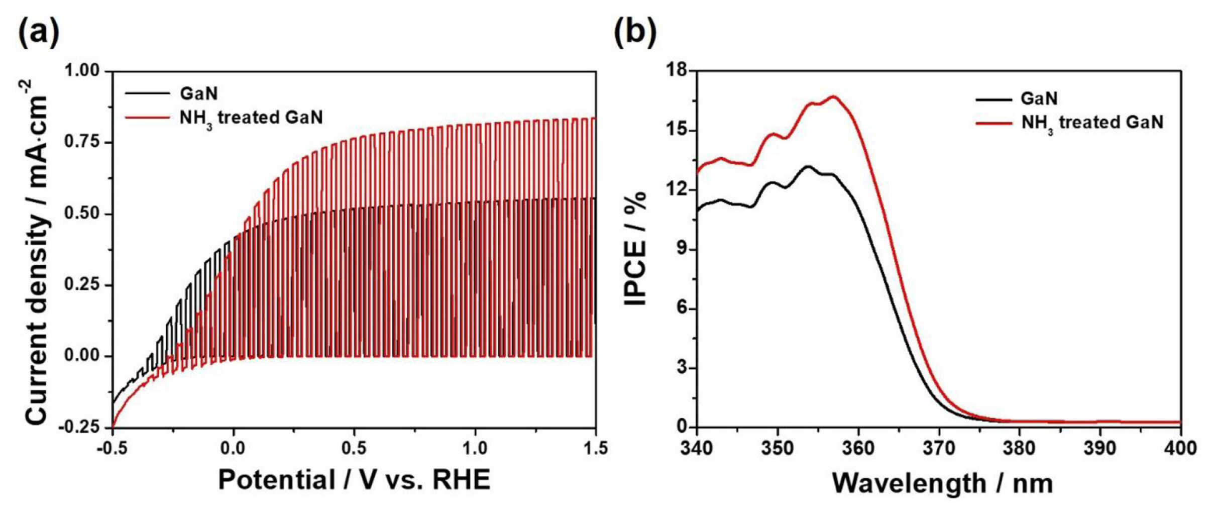
Fig. 3(a) displays chopped voltammograms of the GaN and NH3-treated GaN films measured in 0.5 M NaOH (pH = 13) under on/off light conditions (AM 1.5) to establish the negligible dark leakage current. For the GaN film, the photocurrent densities (J) of approximately 0.35 and 0.5 mA·cm−2 at 0.0 and 1.23 VRHE, respectively, were achieved with an onset potential (Von) of −0.3 VRHE. In contrast, the NH3-treated GaN film exhibited J values of approximately 0.35 and 0.78 mA·cm−2 at 0.0 and 1.23 VRHE, respectively, with a Von of −0.24 VRHE. The NH3-treated GaN film exhibited an approximate 50% improvement in J value in the highly applied potential region with a positive shift of Von, while the GaN film exhibited a more constant J curve in the Von region. This result could be ascribed to the more nanotextured surface structure, newly correlating the defect/trap states to the positive Von shift and the formation of a GaOxN1-x phase, partially blocking the charge recombination reaction.
Fig. 3(b) displays the incident photon-to-current conversion efficiency (IPCE) of the GaN and NH3-treated GaN films measured in 0.5 M NaOH (pH = 13) to describe the extent of J as a function of the wavelength at a potential of 1.23 VRHE. In general, the IPCE value can be described by the following equation (3) [14]:
where J is the photocurrent density (mA·cm−2) and λ is the wavelength of the illuminating light. It was observed that the IPCE profile of both films exhibited similar trends and the NH3-treated GaN film displayed more enhanced IPCE values over the entire photo-responsive wavelength range, with a maximum IPEC value of approximately 17% at a wavelength of 360 nm. This result corresponded to the J values for the LSV curve (J-V curves) in Fig. 3(a). This result again confirmed that the NH3 treatment could boost the J value of the PEC cell, particularly due to the UV wavelength.
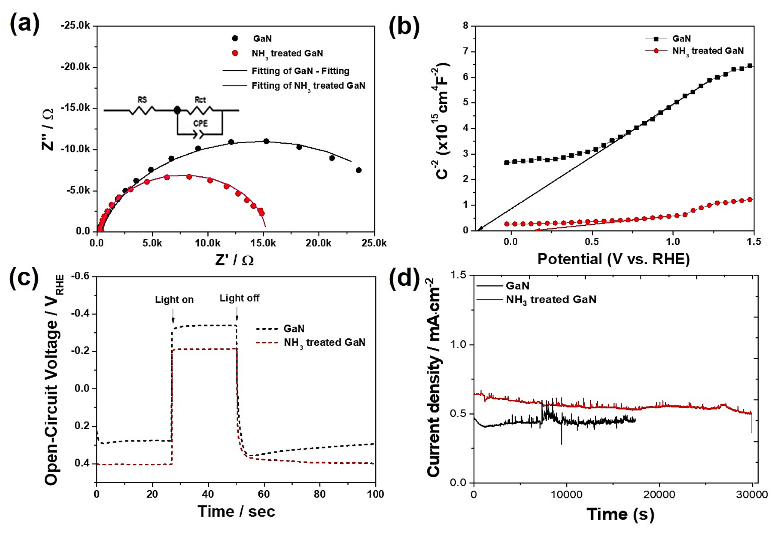
Electrochemical impedance spectroscopy (EIS) was employed to assess the charge transfer/transportation kinetics of the GaN films. Fig. 4(a) displays the Nyquist plots of both films, measured in a deaerated aqueous electrolyte containing 0.5 M NaOH under one sun illumination under an open-circuit potential (OCP) condition. The effects of NH3 treatment on the GaN films were intensively investigated in terms of their effect on the charge transfer/transportation properties. For accurate analysis, the suggested equivalent circuit model (Fig. 4(a) inset) was explored to fit the raw data and provide quantitative values. Herein, RS, RCT, and CPE refer to the series resistance including the ions present in the aqueous electrolyte and the external circuit connection between the electrodes, the charge transfer resistance assigned to the photo-electrode/electrolyte interface, and double layer characteristic, respectively. In more detail, CPE is the capacitance of the electrical double layer between the electrode and electrolyte [15]. Overall, the RS values of both films were similar (~50 Ω), whilst RCT for the pristine GaN film was the largest (~9500 Ω) compared to ~5000 Ω for the NH3-treated GaN film. In the presented Nyquist plots, a decrease in the size of the semicircles for the NH3-treated GaN film represented a smaller RCT, implying that it would be possible to achieve faster interfacial charge transfer and longer lifetimes for photo-induced electron-hole pairs.
The interfacial electrical characteristics of the GaN and NH3-treated GaN films were examined by a Mott-Schottky analysis through EIS measurements in an electrolyte of 0.5 M NaOH (pH = 13), as displayed in Fig. 4(b). To obtain typical Mott-Schottky plots, the measurements were performed in a three-electrode configuration with a modulating applied potential at a frequency of 1 kHz under dark conditions. The extrapolation lines through the x-axis of the M-S plots provide information on the flat-band potential (EFB) of the films. All the photoelectrodes exhibited a positive slope in their d(C−2)/dV, confirming that all films exhibited n-type conductivity. To obtain the quantitative EFB and ND values more accurately, the following equations (4,5) were adapted [16]:
where e0, ɛ, ɛ0, ND, and V are the electronic charge, dielectric constant (~5.3) of the GaN film, vacuum permittivity, carrier density, and applied potential, respectively. In terms of the flat band potential (EFB), the NH3-treated GaN film exhibited a more positive shift in potential from −0.2 to +0.15 V relative to the GaN film, offering significant insights into the lower quasi-Fermi level. This result could be ascribed to the formation of a GaOxN1-x phase as well as the defect/trap state in the interfacial GaN/electrolyte region, caused by the formation of more cracks or crystalline stress as a result of the NH3 treatment. Furthermore, the corresponding carrier density (ND) of the pristine GaN and NH3-treated GaN films were estimated as 4.01 × 10¹⁹ and 9.83 × 1019 cm−3, respectively. The increased donor density was expected to improve the electrical conductivity of the NH3-treated GaN photoanode film, reducing the internal resistance of the photoanode film and forming a favorable element coordination in the modified photoanode. These sites in the interfacial connecting region can act on the cascading medium to mediate the photo-generated holes to the electrolyte under illumination, favorably transferring them to the electrolyte for the faradaic reaction.
For deeper insights into the surface charge transfer phenomenon, the OCP decay was measured as a function of time immediately after the light illumination was abruptly blocked, as displayed in Fig. 4(c). The photovoltage (Vph) estimated through OCPdark–OCPlight was 0.63 and 0.61 V for the GaN and NH3-treated GaN films, respectively, indicating there was no meaningful difference between the films. The average lifetime of each V-t profile by fitting to a biexponential function with two-time constants was calculated using the following equations (6,7) [17,18]:
where τn is the average lifetime and log (2 × τn) is the total half-life. Here, τn values of the photocarriers were estimated as 0.8 and 1.02 s for the GaN and NH3-treated GaN films, respectively. This result confirmed the efficient formation of photo-generated charges against the fast charge recombination surrounding the interfacial region in the NH3-treated GaN film.
To determine the durability of GaN and NH3-treated GaN films, its long-term stability was assessed at 1.23 VRHE, as shown in Fig. 4(d). The NH3-treated GaN film achieved constant photocurrent density for over 8 h, with an average photocurrent density of 0.62 mA·cm−2, demonstrating excellent durability for PEC water oxidation. Furthermore, the durability of bare GaN film was also performed at the same applied potential, which maintains 5 h stability with a photocurrent density of 0.45 mA·cm−2, with abrupt degradation and dissolution over time, dedicating the stable performance of NH3-treated GaN film, as compared to bare GaN film.
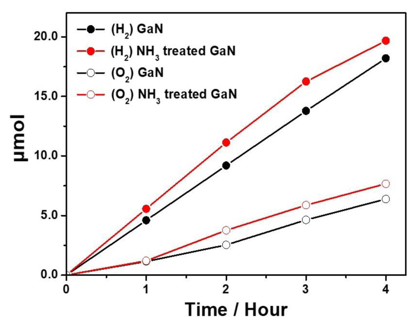
The H2/O2 evolution rate over time was detected using an airtight rubber-corked 120 mL volume of quartz in a PEC cell. The chronoamperometric mode at a constant applied potential of 1.23 VRHE was employed in a 3-electrode system using a customized closed reactor cell. In this system, the use of 0.5 M NaOH (pH = 13) of aqueous solution was explored as an electrolyte under continuous light (one sun) illumination (100 mW·cm−2 with AM 1.5 filter). Fig. 5 presents the amount of evolved H2/O2 gas (μmol) of GaN and NH3-treated GaN films, and their quantitative values are summarized in Table 1, including the Faradaic Efficiency (FE, %). A maximum FEH2 of ~92% was achieved by the NH3-treated GaN film, compared to ~83% for the GaN film. As the time increased to 4 h, a slight decrease in FEH2 was observed and the GaN film exhibited severe FEH2 degradation. Conversely, the FEO2 started at below ~50% and reached 58% after 3 h, then reduced to 56%. Overall, slightly improved FEO2 values were achieved with the NH3-treated GaN film saturated for 3 h. Furthermore, the quantitative H2:O2 ratio detected by GC was compared to reveal a higher H2 generation ratio compared to O2 generation under the situation where the level of FEO2 was lower than FEH2.
In conclusion, the NH3 treatment could cause a new transformation of the native GaOx phase in the GaN film to form an N-Ga-O phase as the blocking layer against the charge recombination process under the beneficial charge transfer process. Furthermore, the surface nanotexturing promoted light absorption as well as the photoactive reacting sites. Therefore, NH3-treated GaN film can boost PEC activity compared to a bare GaN film.
4. Conclusions
In this study, post-treated NH3 annealing was investigated using a bare GaN film in a facile NH3 atmosphere at 900°C. The bare GaN exhibited a highly crystalline wurtzite structure with the (002) plane and the optical bandgap existed at ~3.2 eV. In addition, the NH3-treated GaN film exhibited slightly reduced crystallinity and slightly improved light absorption, probably resulting from the lattice stress or some cracks caused by the excessive N supply. The minor surface nanotexturing created increased surface area, providing electroactive reacting sites. From the surface XPS analysis, the formation of the N-Ga-O phase on the surface region of the GaN film was confirmed to suppress the charge recombination process and cause a positive shift of EFB. Therefore, these effects boosted PEC activity, with J values of NH3 treated GaN film of ~0.35 and ~0.78 mA·cm−2 at 0.0 and 1.23 VRHE, respectively, and an onset potential (Von) of −0.24 VRHE. The approximate 50% improvement of J value in the highly applied potential region with the positive shift of Von could be explained by the increased nanotexturing on the surface structure, the newly formed defect/trap states, correlated to the positive Von shift, and the formation of the GaOxN1-x phase which partially blocked the charge recombination reaction. Therefore, the appropriate post-treatment of the GaN film can boost PEC performance by intimate surface nano-engineering.



 PDF Links
 PubReader
 ePub Link
 Full text via DOI
 Download Citation