


Atomic Force Microscopy (AFM) Tip based Nanoelectrode with Hydrogel Electrolyte and Application to Single-Nanoparticle Electrochemistry
- Kyungsoon Park1,*, Thanh Duc Dinh2,†, Seongpil Hwang2,*
- Received October 23, 2023 Accepted November 6, 2023
- ABSTRACT
-
An unconventional fabrication technique of nanoelectrode was developed using atomic force microscopy (AFM) and hydrogel. Until now, the precise control of electroactive area down to a few nm2 has always been an obstacle, which limits the wide application of nanoelectrodes. Here, the nanometer-sized contact between the boron-doped diamond (BDD) as conductive AFM tip and the agarose hydrogel as solid electrolyte was well governed by the feedback amplitude of oscillation in the non-contact mode of AFM. Consequently, this low-cost and feasible approach gives rise to new possibilities for the fabrication of nanoelectrodes. The electroactive area controlled by the set point of AFM was investigated by cyclic voltammetry (CV) of the ferrocenmethanol (FcMeOH) combined with quasi-solid agarose hydrogel as an electrolyte. Single copper (Cu) nanoparticle was deposited at the apex of the AFM tip using this platform whose electrocatalytic activity for nitrate reduction was then investigated by CV and Field Emission-Scanning Electron Microscopy (FE-SEM), respectively.
- 1. Introduction
- 1. Introduction
Electrochemistry at the nanometer regime has drawn much attention for the characterization of the synthesized nanomaterials [1,2], the better electrocatalysts/ active nanomaterials in electrochemical energy conversion/ storage [3–6], and the electrochemical sensors for various analytes [7,8]. Compared to the conventional macroelectrodes, electrochemistry using nanoelectrodes has tremendous advantages such as enhanced mass-transfer rates, smaller RC constants, enhanced faradaic to capacitive current ratio and negligible influences from solution resistance [9–11]. The understanding of electrochemical properties under the nanoscale domain was mainly conducted using nanoelectrode ensembles (NEEs), which do not provide information on the molecular level but the averaged properties. The structure-activity relationship for electrochemistry, however, requires the electrochemical investigation of single nanoparticles based on collision [12–15], and nanoscale electric contact [16–18], where the role of nanoelectrode should be highlighted. Generally, two major approaches have been used to fabricate the nanoelectrode. First, a conductive nanowire encapsulated by a glass capillary has been used based on laser-assisted pulling, followed by mechanical polishing [19–21]. Second, conventional lithographic techniques have been utilized to fabricate the nanoelectrode. Both approaches have their advantages and disadvantages. For instance, the former is friendly to conventional electrochemical measurements, but it is subtle and complicated. The latter is easy to design but demands a larger amount of time and expense. Even though the electrochemical application of nanoelectrode is fascinating, it is still challenging to find an optimal solution for the fabrication. Consequently, developing a facile and cost-effective method is fundamental to the understanding of nanoelectrode research.Atomic Force Microscopy (AFM) has been one of the standard methods to investigate the surface properties of nanomaterials such as topography [22] and electrical conductivity [23]. Electrochemistry also has been utilized in the AFM system to characterize the electrode surface such as adsorption and initial stage of electrodeposition [24]. Recently, AFM-combined scanning electrochemical microscopy (AFM-SECM) has been developed to acquire both topography and chemical activity [25–27]. The key technology for AFM-SECM is the passivation of conductive AFM tip while maintaining a defined exposure of the working electrode on the nanometer scale. So far, focused ion beam (FIB) milling has been applied to create a hole in the passivation layer such as silicon nitride. However, the surface state of the electrode would largely affect the nature of electrochemistry, making this milling process labor-intensive and expensive to obtain an adequate nanoelectrode.In this paper, we investigated the electrochemistry of nanoelectrode combining commercially available conductive AFM tip with hydrogel electrolyte, whose solid-liquid properties were focused [28]. Specifically, the hydrogel plays a dual role as a liquid electrolyte in electrochemistry and a solid substrate for AFM. Under non-contact mode, when the tip was set to engage with the hydrogel surface, a nanoelectrode was formed at the interfacial region of contact between the electrolyte and conductive AFM tip. Here, the size of the nanoelectrode was easily controlled by a set point of feedback amplitude in the AFM controller. In addition to the study of outer-sphere charge transfer, the modification of a single micro/nanoparticle at the apex of the AFM tip was achieved by Cu electrodeposition. Therefore, our strategy is expected to provide a simple approach for the fabrication of nanoelectrodes through the convergence of conventional devices, which could suppress technological issues for their applications.
- 2. Experimental
- 2. Experimental
- 2.1 Materials
- 2.1 Materials
Agarose (Low EEO, ≥ 99%), ferrocenemethanol (FcMeOH, ≥ 97%), potassium sulfate (≥ 99.0%), potassium chloride (≥ 99.0%), potassium nitrate (≥ 99.0%), sulfuric acid (≥ 99%) and copper (II) sulfate pentahydrate (≥ 98%) were purchased from Sigma-Aldrich. All the chemicals and reagents used in this work were of the reagent grade, and water (≥ 18.2MΩ·cm) was obtained from a Millipore Milli-Q purification system.- 2.2 Preparation of agarose hydrogel for electrochemistry
- 2.2 Preparation of agarose hydrogel for electrochemistry
Agarose solution (8.3 wt% agarose in water) was prepared in a chemically resistant and autoclavable container. The solution in the container was preconditioned in a 90°C water bath for an hour until the agarose was completely dissolved. Air bubbles which would disrupt the gel were eliminated by heating under a microwave (700 W) for 30 s until the solution became viscous and transparent agarose solution. The prepared agarose solution was poured into a plastic mold and cooled down slowly (overnight at room temperature) in a humid chamber. The solidified agarose pad was cut into desired sizes, then, carefully separated from the mold and stored in distilled water. Before electrochemical measurements, the agarose gels were soaked into an aqueous electrolyte of redox molecules and supporting electrolyte for 8 hours to achieve an equilibrium state. For electrochemical measurement, agarose gel containing redox material was fixed on a glass slide using a resin bond.- 2.3 Electrochemical and AFM measurements
- 2.3 Electrochemical and AFM measurements
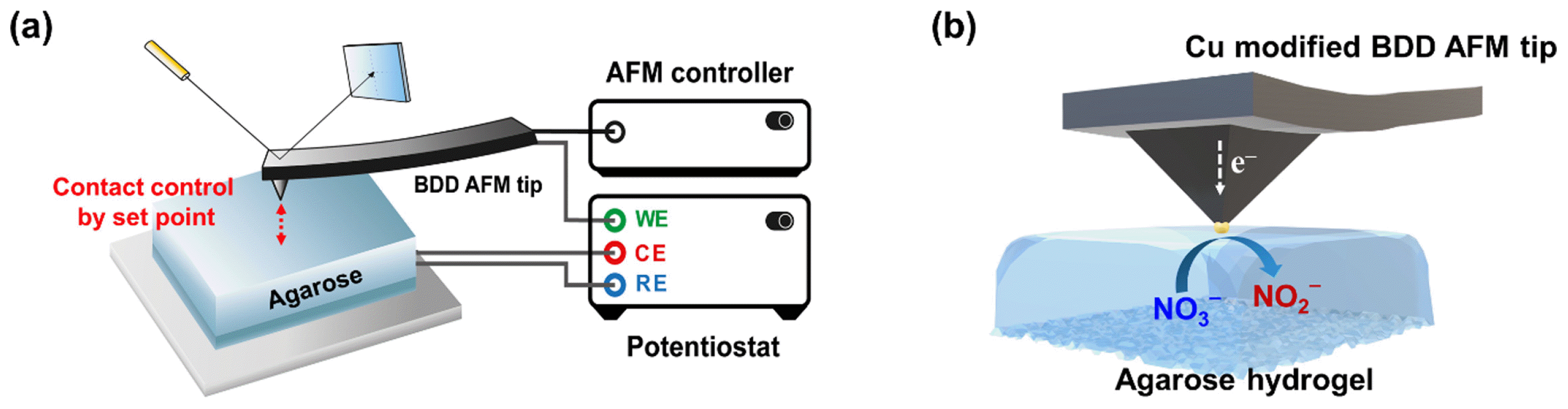
Electrochemical measurements were carried out using a potentiostat (CHI 730E, CH Instruments) and the contact area between the conductive AFM tip and the agarose gel was controlled by the AFM system (NX-10, Park Systems) according to the set point in the non-contact mode. A boron-doped diamond (BDD) coated AFM tip (CDT-NCHR, Nanosensors) with attached conductive wire for electrical contact was used as a working electrode. Meanwhile, a Pt wire and an Ag/AgCl wire were used as counter electrode and quasi-reference electrode, respectively, which were positioned inside the agarose gel. The aqueous electrolyte of 1.0 mM FcMeOH and 1.0 M KCl was employed as a soaking solution to determine the nano-sized contact area between the hydrogel and the conductive tip. The potential for oxidation of FcMeOH (0.4 V vs. Ag/ AgCl) was applied at the BDD AFM tip for the chronoamperometric measurement.- 2.4 Principles of non-contact AFM
- 2.4 Principles of non-contact AFM
In the non-contact mode, the tip oscillates near its resonant frequency (f0). During the movement of the tip, the AFM system monitors intermolecular forces between the tip and sample as feedback signals, which leads to changes in its oscillation frequency and amplitude. When the distance between the AFM tip and the sample surface becomes much closer, the oscillation amplitude becomes smaller than that in free space due to the stronger attraction force. Accordingly, in the non-contact mode of AFM, the interaction between the tip and surface can be adjusted by changing the oscillation amplitude as a set point. So, a low setpoint in this work denotes that the distance between the BDD-AFM tip and the agarose hydrogel is close and the contact area is large.- 2.5 Electrodeposition of Cu and electrocatalytic effect for nitrate reduction
- 2.5 Electrodeposition of Cu and electrocatalytic effect for nitrate reduction
The electrochemical deposition of Cu on the BDD AFM tip was carried out in a similar configuration to the previous cell. Agarose gel was immersed in 0.5 M H2SO4, 50 mM CuSO4 and 0.1 M K2SO4 as a soaking solution, and the CV scans were recorded between 0.1 V to −0.65 V at a scan rate of 50 mV/s. The surface morphology of the electrodeposited Cu on the BDD AFM tip was characterized by field emission scanning electron microscopy (FE-SEM, Carl Zeiss, PLUS II). To confirm the electrocatalytic properties of copper in sensing nitrate ions, various concentrations of KNO3 were used.
- 3. Results and Discussion
- 3. Results and Discussion
Scheme 1(a) illustrates how to fabricate a nanoelectrode by conductive AFM tip with hydrogel electrolyte. Commercially available conductive boron-doped diamond (BDD) coated tip was mounted to the conventional AFM instrument. BDD was chosen as an electrode material because BDD ultramicroelectrode is not widely used despite its outstanding characteristics. The mechanical properties of BDD are incompatible with the UME fabrication based on the pulling method so only the lithographic approach is available. In contrast, the BDD-coated AFM tip is off-the-shelf from various providers. It should be mentioned that our approach is applied to various electrode materials such as Au, Pt, and carbon materials in the shelf of conductive AFM tip. Agarose gel served both as an electrolyte for electrochemistry and a solid-like substrate to define the electroactive area. To fabricate a nanoelectrode, a set point of 12 nm was used for the approach of the BDD tip to hydrogel. To confirm the stable electrical contact between the BDD-AFM tip and agarose hydrogel, the tip current was plotted as a function of time, while the conductive tip under applied potential was approached to the agarose surface (Fig. 1). Before the tip contacted the agarose, the current was negligible. When the apex of BDD made contact with agarose at ca. 15 s, the anodic current surged by both the charging process and the faradaic process. During the subsequent 2 s, the anodic current was recorded as a fluctuating signal probably because of the change at BDD tip/ agarose within the water meniscus. Then, a stable faradaic current was observed. The steady-state current of ca. 2 pA reveals the successful formation of nanoelectrode between the BDD-AFM tip and agarose hydrogel.The electrochemistry of our platform at the nanometer scale was investigated. Fig. 2 shows the cyclic voltammograms (CVs) of conventional BDD AFM tip for the oxidation of ferrocenemethanol (FcMeOH) at various set points. All CVs demonstrate the sigmoidal shape indicating the radial diffusion dominant condition from ultramicroelectrode. The lower the set point was, the larger the faradaic current was observed. This is reasonable because the contact area between the tip and the agarose would be larger according to the lower set point (more interaction). Namely, the tip with the lower set point was pushed more to the elastic hydrogel resulting in the larger contact area. The height of the nanoelectrode depending on the set point of non-contact mode AFM is calculated from the steady-state limiting current, iss, and the mass-transfer resistance for a pyramidal-shaped electrode [29]:Where n is the number of electrons transferred, F is Faraday’s constant, D is the diffusion coefficient of redox reactant, C is the bulk concentration of redox species in solution and a is the height of the nanoelectrode. Diffusion of FcMeOH in agarose gel is almost identical to that in the aqueous phase [28,30]. The estimated heights are 54.8, 75.8, and 231.6 nm for set points of 4, 5, and 6 nm, respectively. It should be mentioned that due to the use of the BDD tip, the electrode surface has a pyramidal shape instead of a common inlaid disk. Therefore, the steady-state current was proportional to nFDCa with a slightly modified proportional constant deviated from 4 in Eq. (1). The nanoelectrode from a conventional AFM tip is successfully fabricated just by a simple change in set point without any further lithographic process or further insulation followed by exposure by such method as focused ion beam.The single nanoparticle of Cu was electrochemically deposited on this nanoelectrode. Hydrogel was filled with the electrolyte containing 50 mM CuSO4, 0.5 M H2SO4 and 0.1 M K2SO4. Then BDD AFM tip was brought in contact under AFM feedback. Fig. 3 shows a representative CV with 1 nm as a set point. The cathodic current corresponds to the reduction of Cu2+ to metallic copper while the anodic current demonstrates the dissolution (oxidation) of the deposited copper. The quantity of Cu using the charge amount integrated from the anodic current is approximately 5.5×10⁻¹⁵ mol numbers corresponding to ca. 200 nm in radius assuming spherical Cu particle. The overpotential for copper deposition seems to be large probably because of weak interaction between Cu seeds and BDD film. To fabricate Cu particles, the potential sweep was stopped at −0.65 V followed by retracting the AFM tip. After slightly rinsing, the apex of the AFM tip was investigated through FE-SEM. Fig. 4(A,B) are the images before and after Cu electrodeposition with 1 nm as a set point, respectively. Urchinlike Cu particles were electrochemically deposited as shown in Fig. 4(B), where each spike was ca. 100 nm in width. With a larger set point of 13 nm (in other words, the contact area decreased), Fig. 4(D) shows the formation of Cu nanorod at the apex whose size is ca. 90 nm in width and 200 nm in length. The control of morphology and shape is out of the scope of our paper as the well-controlled fabrication of the electrodeposited nanoparticle is still challenging dependent on various parameters [31–33]. Nonetheless, Cu nanomaterials were successfully fabricated and immobilized at the apex of the AFM tip for further characterization of electrocatalytic properties.Copper-based materials have been investigated as electrocatalysts for the reduction of nitrate anion [34,35], which has drawn much attention as a treatment of water contaminated by fertilizer and a sustainable generation of ammonium. As depicted in Scheme 1(b), the electrocatalytic reduction of nitrate by Cu nanomaterials was characterized by bringing the Cu-modified AFM tip into contact with the agarose gel containing nitrate anions. Fig. 5 shows the linear sweep voltammograms of urchin-like copper-modified BDD AFM tip in the presence of nitrate anion. In the absence of nitrate anion, the cathodic current was negligible because both BDD and Cu show poor catalytic activity for hydrogen evolution reaction (HER). Additional cathodic peaks corresponding to nitrate reduction appeared when nitrate was added to the identical condition with the concentrations from 100 mM to 5 mM as shown in Fig. 5. Herein, the first reduction stage of nitrate ions was observed at −0.83 V, followed by the second reduction wave indicating the consecutive reduction as follows [36,37];Nitrate reduction is in good accordance with the previous report with Cu-Pt nanostructure under the identical conditions, while the Cu particles did not show any traces of the spontaneous oxidation of Cu. Here, the urchin-like Cu nanoparticles acted as the ultramicroelectrode so that the steady-state current was also observed for the first nitrate reduction due to the fast mass transport. This radial diffusion, however, may enhance the transportation of the generated nitrite from the catalyst surface to the bulk solution resulting in the negative shift of the second reduction. These results imply that the electrocatalytic activity of a single nanoparticle may depend on the size not only from the catalytic activity itself but also from the mass transport of the reactant and product. Although further examination of this phenomenon is out of the scope of our paper, we concluded that our approach based on conducting AFM tip with hydrogel paves a new approach to characterize the electrocatalytic activity of a single nanoparticle.
- 4. Conclusions
- 4. Conclusions
Nanoelectrodes with controlled active areas were developed using commercially available BDD-coated AFM tip and agarose hydrogel as solid electrochemical media. The contact area between the BDD AFM tip and the agarose surface can be adjusted by measuring oscillation amplitude as a set point in the non-contact mode of AFM. The CVs of the redox probe demonstrated that the radial diffusion was observed at our nanoelectrode and the electrode size could be determined from steady-state currents to be tens to hundreds of nm. For the application of the single nanoparticle as an electrocatalyst, the electrochemically deposited Cu nanoparticle on our nanoelectrode was successfully investigated using CV and FE-SEM. In addition, the electrocatalytic activity of Cu particles was confirmed by two-step consecutive nitrate reduction using linear sweep voltammetry. This result suggests that the catalytic activity of a single nanoparticle is not affected only by size but also by the diffusional properties of reactants and products. Our work demonstrated that the commercial AFM and agarose can be used as a new method for the simple fabrication of nanoelectrodes and studying the electrocatalytic activity of a single nanoparticle.
- Acknowledgments
- Acknowledgments
S. H. acknowledges the support from Basic Science Research Program through the National Research Foundation of Korea (NRF) grant funded by the Korea Government (MSIP) (No. RS-2023-00209181). This work was supported by a Korea University Grant. Also, K.P. acknowledges the support from Basic Science Research Program to Research Institute for Basic Sciences (RIBS) of Jeju National University through the National Research Foundation of Korea (NRF) funded by the Ministry of Education. (2019R1A6A1A10072987). This research was also supported by the Basic Science Research Program through the National Research Foundation of Korea (NRF) funded by the Ministry of Education (NRF-2022R1I1A3072996).
Fig. 1
Chronoamperometric curve was obtained as the BDD AFM tip approached the 1 mM FcMeOH and 1.0 M KCl containing agarose hydrogel at 0.4 V vs. Ag/AgCl. This curve was measured with a set point of 12 nm.
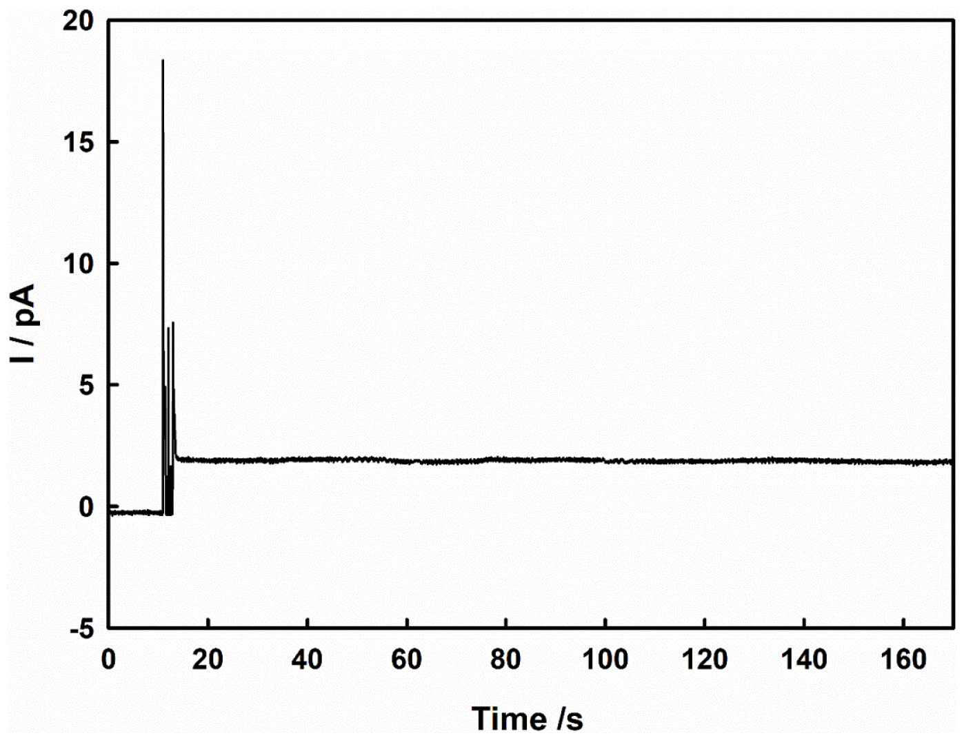
Fig. 2
Cyclic voltammograms of BDD AFM tip on the agarose hydrogel containing 1 mM FcMeOH and 1.0 M KCl corresponding to different set points. Set point: (a) 4 nm, (b) 5 nm, (c) 6 nm. Scan rate is 0.02 V/s.

Fig. 3
Cyclic voltammograms of BDD AFM tip for electrochemical Cu deposition on agarose hydrogel containing 0.5 M H2SO4, 50 mM CuSO4, 0.1 M K2SO4. Scan rate: 0.05 V/s, set point: 1 nm. The potential sweep was stopped at the third sweep for Cu deposition.
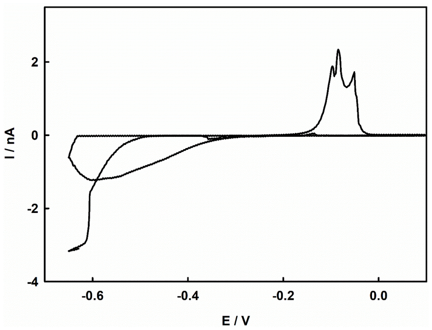
Fig. 4
FE-SEM images of Cu deposited BDD AFM tips depending on the set points. Images of (A) bare BDD AFM tip, (B) 1 nm as a set point, (C) 13 nm as a set point, and (D) a magnified image of the apex of (C).
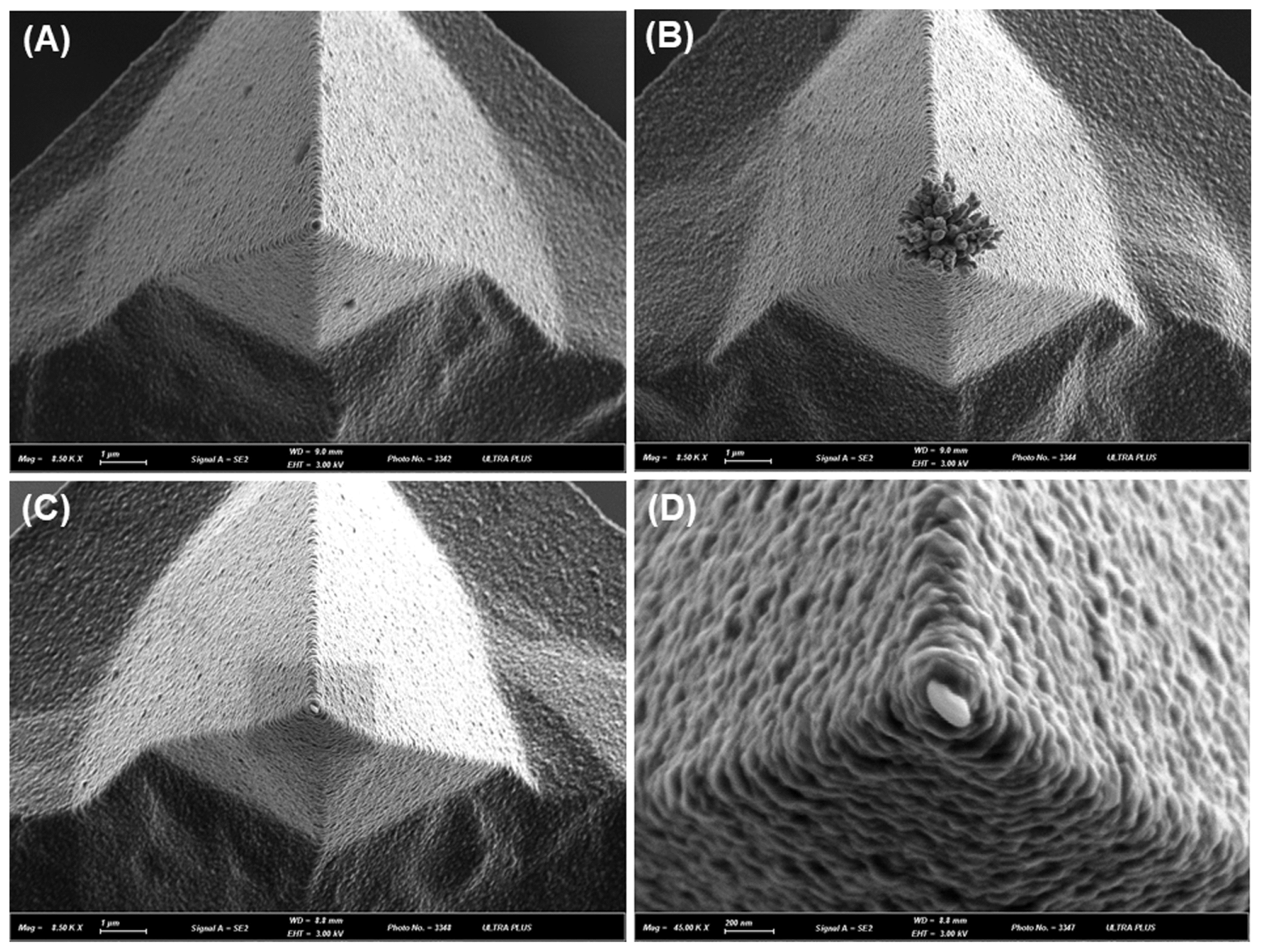
Fig. 5
Linear sweep voltammograms of nitrate reduction using Cu-modified BDD AFM tip at different concentrations of KNO3 containing 0.5 M KCl and (a) 0 mM, (b) 0.1 mM, (c) 1.0 mM, and (d) 5.0 mM KNO3. Scan rate: 0.05 V/s. In (b–d), tip (B) in Fig. 4 was used as an electrocatalyst for nitrate reduction.

Scheme 1
(a) Schematic illustration of the contact between the BDD AFM tip and hydrogel corresponding to the set point of AFM, and (b) electrocatalytic nitrate reduction using Cu modified AFM tip at agarose hydrogel as a solid electrolyte.
- REFERENCES
- REFERENCES
References
[1] F. Zhang, M. A. Edwards, R. Hao, H. S. White and B. Zhang, J. Phys. Chem. C., 2017, 121(42), 23564–23573.
[Article][3] Q. Chen, L. Luo, H. Faraji, S. W. Feldberg and H. S. White, J. Phys. Chem. Lett., 2014, 5(20), 3539–3544.
[Article][4] Y. Yu, Y. Gao, K. Hu, P.-Y. Blanchard, J.-M. Noël, T. Nareshkumar, K. L. Phani, G. Friedman, Y. Gogotsi and M. V. Mirkin, ChemElectroChem., 2015, 2(1), 58–63.
[Article][5] J. Clausmeyer, J. Masa, E. Ventosa, D. Ohl and W. Schuhmann, Chem. Commun., 2016, 52, 2408–2411.
[Article][6] H. B. Aiyappa, P. Wilde, T. Quast, J. Masa, C. Andronescu, Y.-T. Chen, M. Muhler, R. A. Fischer and W. Schuhmann, Angew. Chem. Int. Ed., 2019, 58(26), 8927–8931.
[Article][8] D.-S. Kim, E.-S. Kang, S. Baek, S.-S. Choo, Y.-H. Chung, D. Lee, J. Min and T.-H. Kim, Sci. Rep., 2018, 8, 14049.[12] X. Xiao, F.-R. F. Fan, J. Zhou and A. J. Bard, J. Am. Chem. Soc., 2008, 130, 16669–16677.
[Article][15] W. Xu, G. Zou, H. Hou and X. Ji, Small., 2019, 15(32), 1804908.[16] S. M. Oja, D. A. Robinson, N. J. Vitti, M. A. Edwards, Y. Liu, H. S. White and B. Zhang, J. Am. Chem. Soc., 2017, 139(2), 708–718.
[Article][18] W. Wei, T. Yuan, W. Jiang, J. Gao, H.-Y. Chen and W. Wang, J. Am. Chem. Soc., 2020, 142(33), 14307–14313.
[Article][24] S. Manne, P. K. Hansma, J. Massie, V. B. Elings and A. A. Gewirth, Science., 1991, 251(4990), 183–186.
[Article][26] A. Kueng, C. Kranz, A. Lugstein, E. Bertagnolli and B. Mizaikoff, Angew. Chem. Int. Ed., 2003, 42(34), 3996–4028.[27] C. Kranz, A. Kueng, A. Lugstein, E. Bertagnolli and B. Mizaikoff, Ultramicroscopy., 2004, 100(3–4), 127–134.
[Article][31] S. E. Kleijn, S. C. S. Lai, M. T. M. Koper and P. R. Unwin, Angew. Chem. Int. Ed., 2014, 53(14), 3558–3586.
[Article][35] Y. Wang, W. Zhou, R. Jia, Y. Yu and B. Zhang, Angew. Chem. Int. Ed., 2020, 59(13), 5350–5354.
[Article][36] Z. Mumtarin, M. M. Rahman, H. M. Marwani and M. A. Hasnat, Electrochim. Acta., 2020, 346, 135994.
[Article][37] T. Ren, K. Ren, M. Wang, M. Liu, Z. Wang, H. Wang, X. Li, L. Wang and Y. Xu, Chem. Eng. J., 2021, 426, 130759.
[Article]