Low-Temperature Solution Process of Al-Doped ZnO Nano-flakes for Flexible Perovskite Solar Cells
Article information
Abstract
Herein we report on the selective synthesis and direct growth of nanostructures using an aqueous chemical growth route. Specifically, Al-doped ZnO (AZO) nanoflakes (NFs) are vertically grown on indium tin oxide (ITO) coated flexible polyethylene terephthalate (PET) sheets at low temperature and ambient environment. The morphological, optical, and electrical properties of the NFs are investigated as a function of the Al content. Furthermore, these AZO-NFs are integrated into perovskite solar devices as the electron transport layer (ETL) and the fabricated devices are tested for photovoltaic performance. It was determined that the doping of AZO-NFs significantly increases the performance metrics of the solar cells, mainly by increasing the short-circuit current of the devices. The observed enhancement is primarily attributed to the improved conductivity of the doped AZO-NF, which facilitates charge separation and reduces recombination. Further, our flexible solar cells fabricated through this low temperature process demonstrate an acceptable reproducibility and stability when exposed to a mechanical bending test.
1. Introduction
In recent years, photovoltaic research has witnessed a rapid emergence of hybrid organic-inorganic perovskite materials and devices based upon this material. With a generic chemical formula of CH3NH3PbI3, this material possesses important merits including its direct band gap, large absorption coefficient, and high carrier mobility, in addition to the possibility of being deposited using simple, low-cost processes such as spin coating or dip coating [6,11].
To date, the most widely adapted perovskite solar cells (PSC) have a device configuration where the light absorber (perovskite) is placed between the carrier-selective electron- and hole-transport layers (ETLs and HTLs). It has been reported that devices can perform well when the HTL is entirely absent [1,15,19,24,25], whereas the ETL must be present to achieve high power conversion efficiency (PCE) [8,9,13,27]. The ETL of PSC is typically an n-type semiconductor (metal oxide) nanostructure that allows electron injection from the perovskite to the metal oxide. The most common metal oxide used is mesoporous TiO2 [4,32]. However, TiO2 has low electron mobility, which can create unbalanced charge transport in the perovskite. Further, the high temperature associated with sintering a TiO2 mesoporous framework (>400°C) to obtain a high-quality crystallization is a substantial shortcoming that limits its applications to temperature-sensitive substrates such as plastics [17]. ZnO has been considered as one of the most promising alternative materials to replace conventional TiO2 owing to its advantages including higher bulk electron mobility with a suitable band gap and flexibility in morphology controlling, in addition to low processing temperatures [36]. The substitution of TiO2 by ZnO as an ETL has been considered as one of most promising alternatives to reduce production cost and expand the variety of substrates for the perovskite-based solar cells [18,28].
Most recently, ZnO nanostructures with nanoplate-like morphologies have been employed to fabricate PSC because they are believed to improve device performance by suppressing light reflection and increasing light scattering. Furthermore, they possess a large surface-to-volume ratio, and when integrated with the perovskite absorber, can provide a direct continuous pathway for electron transport with minimal recombination [10,20,22,23,36]. In this regard, several previous reports focused on integrating one-dimensional (1D) ZnO (e.g., nanowires, nanorods, or nanotubes) with PSCs and different functional nanostructured-based devices have been successfully demonstrated [3, 14, 21, 35]. Unfortunately, the devices based on these ZnO nanostructures have achieved modest performance. Possible reasons could be: (i) the size of the 1D-ZnO is considerably smaller than the wavelength of the incident light, which causes optical loss via the random scattering of the incident light, (ii) 1D-ZnO arrays are overly dense, resulting in an insufficient filling fraction and low photon absorption efficiency, (iii) low interfacial area between the 1D-ZnO and the active layer, (iv) low electron injection efficiency, and (v) poor conductivity of the ZnO. Undoubtedly, many great challenges remain in seeking a feasible route to improve light absorption of 1D-ZnO nanostructured solar devices. It is anticipated, however, that these disadvantages can be overcome by developing novel ZnO nanomaterials that have controlled and specific morphology adaptable to PSCs.
As generally known, vertically aligned, highly ordered ZnO nanostructures with good crystallinity and uniform distribution are required for efficient PSCs. Further, high device performance is always accompanied by higher dimensional ZnO nanostructures with larger specific surface areas [16]. In principle, compared with nanorods or nanowires, 2-dimensional (2D) nanostructures such as nanoflakes (NFs) offer numerous benefits: (i) large planes that are greater than the wavelength of the incident light, (ii) vertical configuration that guides the direction of light into devices, and (iii) large interfacial area when in contact with the active layer that facilitates electron transfer. Based on these considerations, 2D ZnO materials appear to be promising candidates for the fabrication of efficient nanostructured-based solar cells. Interestingly, this hypothesis was recently confirmed in a practical work, where solar cell performance was demonstrated to be improved significantly by assembling nanoflakes as a photoanode into the devices [33]. Moreover, as the electron transfer is solely determined by the electrical characteristic of ZnO nanostructures, it is assumed that the increased ZnO conductivity results in higher performance. Previous publications demonstrated that the electrical conductivity of ZnO nanostructures can be improved by chemically modifying these materials with other elements such as gallium (Ga) [26], indium (In) [2], and aluminum (Al) [31]. Notably, Al-doped ZnO (AZO) nanostructures are capable of attaining the highest electrical conductivity without deterioration in optical transmission [34].
Herein we report on a controllable synthesis of ZnO nanostructures with flake-like morphologies. We demonstrate a solution process to directly deposit 2D AZO nanostructures onto indium tin oxide (ITO) coated flexible polyethylene terephthalate (PET) sheets at low temperature. Consequently, vertically aligned AZO-NFs are directly well formed from an aqueous solution. The changes in the structure, microstructure, and electrical properties are examined as a function of Al doping level in the precursor. Moreover, these AZO-NFs are integrated into regular-type perovskite solar devices as an ETL and are then tested for the photovoltaic (PV) response. It is demonstrated that the performance of the AZO-based devices is dramatically increased with Al content.
2. Experimental
Fig. 1(a) displays the schematic structure of the PSC fabricated in this work. In detail, the ITO/PET substrates are cleaned with detergent, acetone, and isopropyl alcohol (IPA) under ultra-sonication, followed by a nitrogen purge and drying in an oven. A 5 mM solution of Zn(CH3COO)2·2H2O (Sigma-Aldrich) in IPA is spin-coated onto the substrates at 2,000 RPM for 30 s. These films are then calcinated at 125°C on the hot plate for 30 min to form ZnO seed layers.
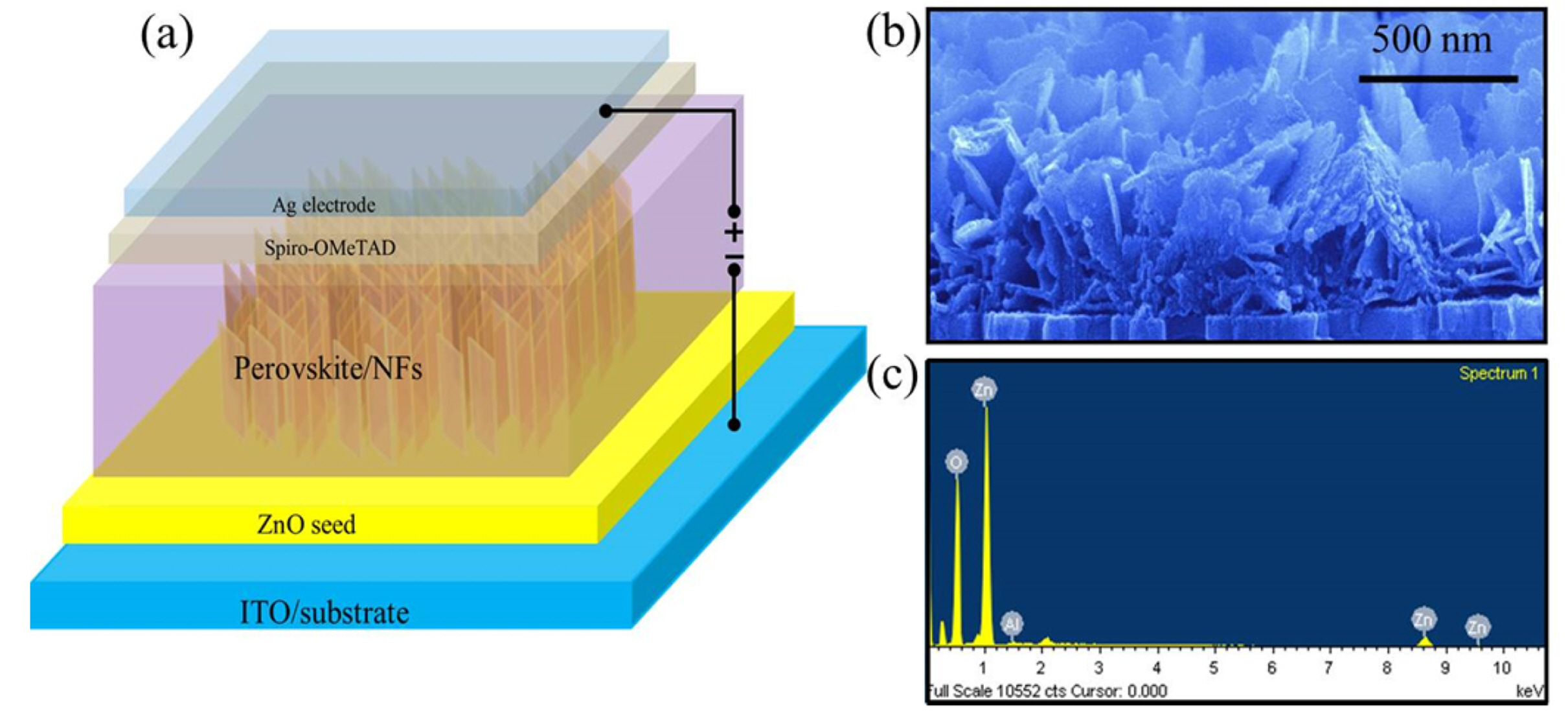
(a) Schematic structure of typical solar devices based on AZ-NF arrays. (b) Cross-sectional FE-SEM images of AZ1-NF array fabricated on ITO-coated PET substrate. (c) EDS spectrum analysis of AZ1-NFs.
Then, AZO-NFs are grown on the seed layers. Zn(CH3COOH)2·2H2O (99%) and Al(NO3)3·9H2O (99%) are used as raw materials for the solution preparation. Two reagents are weighed to have the following batch compositions: Zn(CH3COO)2·2H2O + x Al(NO3)3·9H2O, with x = 0.00, 0.01, 0.02, 0.05, 0.08, and 0.10 (molar ratio; hereinafter abbreviated as AZ0, AZ1, AZ2, AZ3 AZ4 AZ5, respectively), and are dissolved in 10 mL ultrapure water while the concentration is maintained constant at 1.0 M. 8M NaOH was slowly added and mixed with the precursor solution (volume ratio = 1:1) and the mixture is stirred until the color becomes transparent. The resulting solutions are used as the precursor solution for the deposition of the nanoflakes.
After the growth of the AZO-NFs, the substrates are washed with deionized water and IPA for 5 min to remove the residues, followed by calcinations on a hot plate at 125°C for 1 h. The heights of the AZO-NF arrays were approximately 480-520 nm by SEM cross-sectional observation as indicated in Fig. 1(b).
Details of the fabrication and characterization of PSC on the AZO-NF substrates are described in our previous report [11].
3. Results and Discussion
Using aqueous chemical growth, ZnO NFs are grown, which function as the ETL in PSC. As the microstructure of ETL is correlated with the fundamental properties of their devices, a suitable morphology of NF films is primarily required to ensure the reliability of the solar devices. The mechanism of 2D ZnO nanostructure formation from an aqueous solution was previously reported elsewhere [12], where a series of chemical reactions, nucleation, and growth processes were described. The elemental composition of NFs using EDS analysis displayed in Fig. 1(c) confirms the co-existence of Al and Zn elements in the materials.
In Fig. 2, the morphological change of the ZnO nanostructures with Al doping level (x = 0.00-0.10) is displayed. It can be clearly observed that densely packed nanostructure arrays have grown over the ZnO seed layer with an ultrathin plate-like morphology for all compositions. The growth direction of the AZO-NFs is mainly vertical to the underlying substrate. Furthermore, an abundance of empty voids can be observed among the AZO-NFs, where perovskite materials can fill during device fabrication. With increasing Al concentrations, both the density and average size of the AZ NFs gradually decrease, except AZ5, which indicates a minimal increased size. This is consistent with a previous work [7], where AZ NFs were grown onto glass substrates for use in inverted solar cells. Further, it would appear that the Al-doped NFs are better aligned compared with the non-doped NFs.
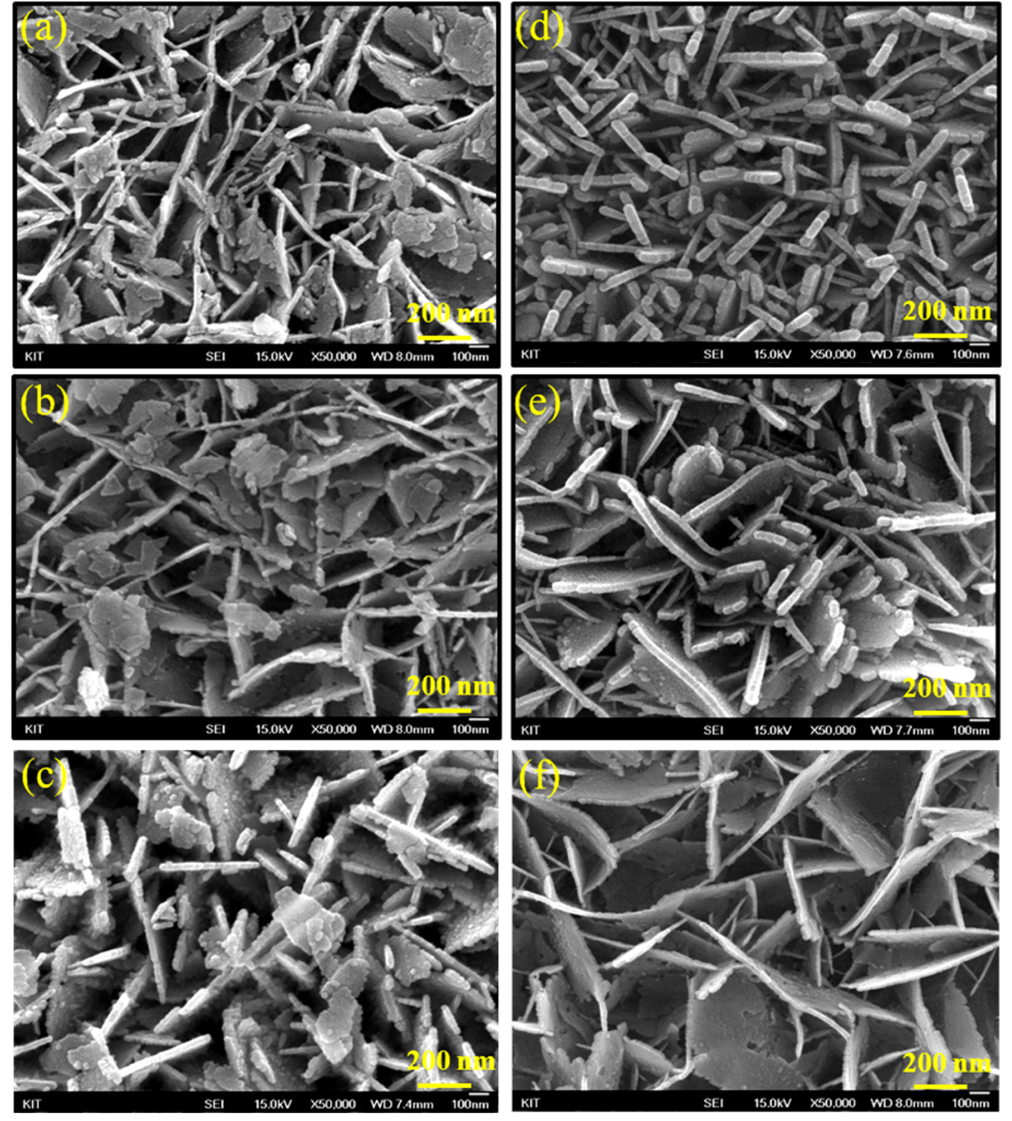
Top view FE-SEM observation of as-grown AZ-NF array system: (a)-(f) AZ0-AZ5, obtained from aqueous solutions with different Al doping concentration.
In Fig. 3, the XRD spectra of the AZO-NFs prepared at different Al concentrations are displayed. Fig. 3 indicates the major peaks of the undoped ZnO-NFs (AZ0) appearing at 2θ = 31.87°, 34.45°, and 36.31°, which were assigned to the (100), (002), and (101) planes of the hexagonal wurtzite ZnO phase, respectively (referenced to hexagonal wurtzite structure with the JCPDS card No 36-1451). The (101) peak indicates the highest intensity, indicating clearly the preferential orientation of the ZnO film. A similar XRD pattern characteristic and peak intensities were demonstrated for all Al-doped samples (AZ1-AZ5). However, as Al doping increases, diffraction peaks shift systematically toward higher values, as can be clearly observed in Fig. 3(b), which can be attributed to the substitution of Al3+ ions for Zn2+ ions in the ZnO lattice during the growth. As the ionic radius of the Al3+ cation (0.54 Å) is smaller than that of Zn2+ cation (0.74 Å), the substitution of Al3+ at the Zn2+ site therefore leads to a reduction of the lattice parameter in the ZnO phase and thus results in the peak shift [5]. This observation also reconfirms that the Al atoms are successfully doped into the ZnO crystals during the growth process. Furthermore, the increased strain in the AZO explains the observation that the size of the AZ NFs is decreased with increasing Al content, as observed in Fig. 2.

X-ray diffraction analysis of AZ-NF arrays annealed at 150°C, as a function of the Al-doping concentration.
In Fig. 4, photoluminescence (PL) spectroscopy was used to compare the relative efficiency of electron- and hole-extraction from the perovskite. Fig. 4(b) displays the PL spectrum of the CH3NH3PbI3 film deposited on bare glass, non-doped, and AZO-NFs. The PL peak at 770 nm is consistent with previous reports of emission from CH3NH3PbI3 [29,30]{Wehrenfennig, 2014 35 /id;Tvingstedt, 2014 36 /id} and the peak positions for all samples are identical. Compared with the perovskite film on bare glass, a significant PL quenching is observed for the perovskite film deposited on the ZnO nanoflakes. This indicates the charge extraction across the interface between the perovskite and ZnO nanoflakes [36]. Compared with the non-doped ZnO, the PL of the perovskite/AZO is further quenched. This is indicative of more effective carrier extraction and reduced recombination, which helps to improve performance of PSC. Furthermore, microscopic observations of the perovskite/ZnO with different Al doping indicate no meaningful difference in surface morphology. We therefore exclude the effect of the perovskite morphological differences on the PL spectra and thus the device performance.
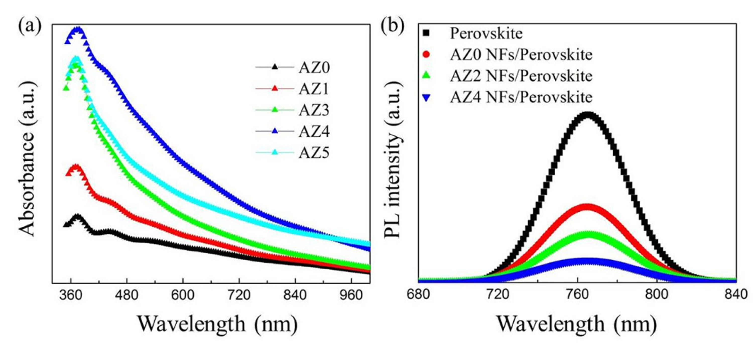
(a) Absorption spectra of non-doped and Al-doped ZnO-NF arrays, annealed at 150°C. (b) Steady-state PL spectra of perovskite films on bare glass, non-doped, and Al-doped ZnO-NF arrays.
Using the AZO-NFs as the ETL, PSC are fabricated by depositing spiro-MeOTAD as the hole transport layer and, finally, a thin Ag layer as the electrode. Fig. 6 displays the current-voltage (I-V) characteristics of the solar cells. In the I-V curves, the effect of Al doping is mainly manifested in the short-circuit current (Jsc). With no doping (AZ0), the Jsc value is significantly lower than the maximum value obtainable with the perovskite material (approximately 20 mA/cm2). This indicates that the charge separation and extraction by the non-doped ZnO is not sufficiently fast that electron-hole recombination results in a reduced Jsc. However, as the Al doping in the ZnO NF is increased, the short-circuit current is increased to as high as approximately 14 mA/cm2. This indicates that electron-hole recombination is significantly reduced on the doped ZnO, likely because of the increased conductivity of highly doped ZnO NF and fast charge extraction. When we use the TiO2 nanoparticle-based cells as a benchmark, the AZO-based cells demonstrate lower performance. This is likely because the AZO-NFs are relatively large and some portion is in contact with the HTL layer, as indicated in the inset to Fig. 7(b), reducing Jsc and Voc. We also fabricated perovskite/ZnO NF solar cells on flexible substrate and performed a mechanical bending test (Fig. 7). The results demonstrate that the flexible solar cells fabricated on a flexible substrate can withstand at least 30 bending cycles without significant loss performance (Fig. 7). After continued bending cycles, the cell performance demonstrated a sudden decrease. We ascribe this degradation to the crack formation in the device structure, as indicated in the inset to Fig. 7(b).

J-V characteristics of PSCs assembled by 2D nanostructured photoanode prepared under different Al doping level. (a) Represented J-V curves of different structured photoanode under simulated AM1.5, 100 mW cm-2 solar irradiation. Inset indicates typical flexible ITO/AZ-NFs/CH3NH3PbI3/spiro-OMeTAD/Ag solar cell at steady state. (b, c) Parameters of PSCs extracted from J-V measurement. (d) Histograms of device performance (PCE) measured for 75 separate ITO/AZ-NFs/CH3NH3PbI3/spiro-OMeTAD/Ag devices. The Gaussian fits are provided as a guide to the eye.
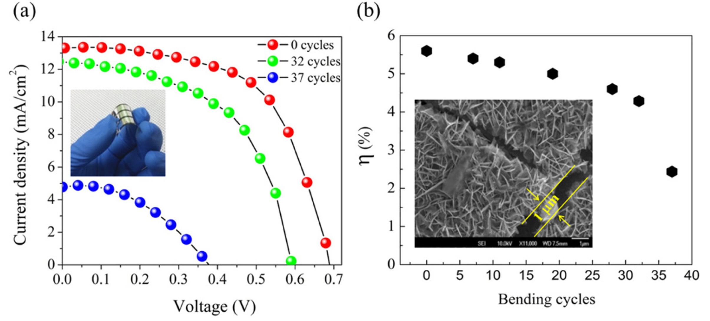
(a) J-V curves of PSCs made by AZ4 after 0, 32, and 37 bending cycles. Inset: typical flexible ITO/AZ-NFs/CH3NH3PbI3/spiro-OMeTAD/Ag solar cell at bending state. (b) Stability of the flexible solar cell under bending at the bending radius of 1.0 cm. Insert indicates cracks of AZ-NF array after 32 bending cycles.
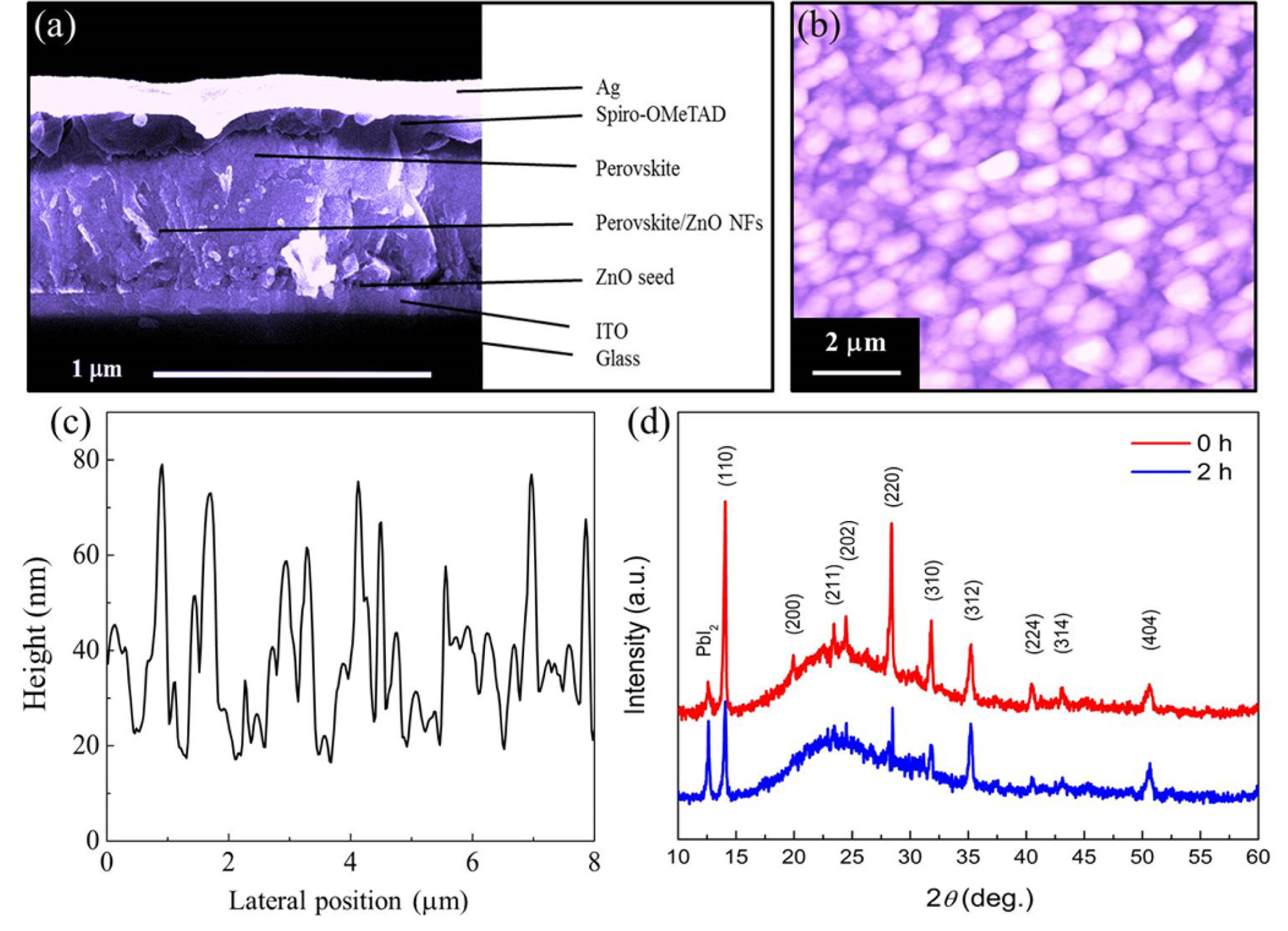
(a) Cross-section SEM image of PSC device based on CH3NH3PbI3 on AZ4-NF arrays. (b, d) AFM topographic image and X-ray diffraction of CH3NH3PbI3 deposited on AZ4-NF arrays. (c) Line profile measured by Scanning Probe Image Processor (SPIP) program for CH3NH3PbI3 film, where the morphology in Fig. 5b was observed.
4. Conclusions
We fabricated flexible PSCs based on flake-like AZO nanostructures with controllable morphology using an aqueous chemical growth route. The effects of the electrical property and morphology characteristics of flake-like AZO nanostructures on the performance of the PSC devices were investigated. It was determined that the PCE of the PSC devices depends critically on the size of the AZO nanostructures and the interface area between the flake-like AZO nanostructures and the active layer. These results suggest that the flake-like AZO nanostructures can be a promising potential candidate in different photovoltaic and optoelectronic applications to improve device performance.
Acknowledgements
This paper was supported by Kumoh National Institute of Technology