Applications of Scanning Electrochemical Microscopy (SECM) Coupled to Atomic Force Microscopy with Sub-Micrometer Spatial Resolution to the Development and Discovery of Electrocatalysts
Article information
Abstract
Development and discovery of efficient, cost-effective, and robust electrocatalysts are imperative for practical and wide-spread implementation of water electrolysis and fuel cell techniques in the anticipated hydrogen economy. The electrochemical reactions involved in water electrolysis, i.e., hydrogen and oxygen evolution reactions, are complex inner-sphere reactions with slow multi-electron transfer kinetics. To develop active electrocatalysts for water electrolysis, the physicochemical properties of the electrode surfaces in electrolyte solutions should be investigated and understood in detail. When electrocatalysis is conducted using nanoparticles with large surface areas and active surface states, analytical techniques with sub-nanometer resolution are required, along with material development. Scanning electrochemical microscopy (SECM) is an electrochemical technique for studying the surface reactions and properties of various types of electrodes using a very small tip electrode. Recently, the morphological and chemical characteristics of single nanoparticles and bio-enzymes for catalytic reactions were studied with nanometer resolution by combining SECM with atomic force microscopy (AFM). Herein, SECM techniques are briefly reviewed, including the AFM-SECM technique, to facilitate further development and discovery of highly active, cost-effective, and robust electrode materials for efficient electrolysis and photolysis.
1. Introduction
Production of hydrogen or hydrocarbons, as sustainable energy vectors, from the electrolysis of water via electrocatalytic or photosynthetic routes has remained a formidable challenge for more than 30 years [1-3]. Since Nicholson and Carlisle first demonstrated water electrolysis in 1800, extensive studies have been undertaken to develop highly active, inexpensive, and durable electrocatalysts for hydrogen production from water splitting [4]. The photoelectrochemical (PEC) production of hydrogen with efficient solar-to-chemical energy conversion (>10%) has also been pursued using various photoelectrodes or buried-junction photovoltaic cells [5,6]. Judicious electrocatalyst selection is crucial for achieving high electrochemical or thermodynamic conversion efficiency for the production of hydrogen from water splitting reactions. Electrocatalysts minimize the overpotentials required for the two innersphere reactions (reactions (1) and (2)), respectively, involved in water splitting for hydrogen evolution (HER) and oxygen evolution (OER) [7].
Cathode: 2H+ + 2e− → H2 (E0 = 0 V vs. RHE, reaction 1)
Anode: 2H2O → O2 + 4H+ + 4e− (E0 = 1.23 V vs. RHE, reaction 2)
Net Reaction: 2H2O → 2H2 + O2 Cell voltage = −1.23 V
Here, RHE refers to the reversible hydrogen electrode, used as a reference electrode in electrochemistry.
Noble metals such as Pt, Ru, and Co and their oxides are known as excellent catalysts for the HER and OER; however, the industrial application of such metals and oxides is not feasible given the limited material resources [8]. To meet the requirements for practical water electrolysis and photolysis, the discovery and development of inexpensive and active metal electrocatalysts, including semiconducting light absorbers, remain imperative. Mechanistic understanding of the role of the developed materials in the relevant reactions must also be achieved to further maximize the catalytic activity of the materials in a given system [9-11]. The activity of metal catalysts in complex multi-electron transfer reactions, i.e., the HER and OER, is not only determined by the intrinsic properties of the catalysts, but is also significantly affected by the interactions between the catalysts and their support electrodes [10]. For example, IrO2, RuO2, and Co3O4 are known as excellent catalysts for the OER on conductive substrates, whereas Pt shows less activity toward the OER than the aforementioned congeners [12]. However, the OER activity of Pt for the photooxidation of water was higher than that of IrO2 or Co3O4 on a semiconducting metal oxide support under UV-visible irradiation [12]. In the case of nanoparticle electrocatalysts, a reverse order of the OER activity was suspected because of the dependence of the activity on the surface structure of the support material, or because of different electronic and adsorbate interactions between the catalyst particles and support substrates. In situ investigation of ultra-small catalysts is therefore essential for the discovery, development, and understanding of electrocatalysts and/or photoactive materials for complex reactions during electrolysis or photolysis.
Herein, we briefly review the application of scanning electrochemical microscopy (SECM) itself and of SECM coupled with atomic force microscopy (AFM) as versatile tools for studying electrode surfaces on the sub-nanometer scale [12,13]. SECM has been used to investigate various electrochemical reactions and electrode surfaces under diffusion-limited reaction conditions using a small probe electrode [12,14-23]. The spatial and temporal resolution of SECM depends on the size of the probe electrode employed in the investigation, as described below [12]. Various approaches have been implemented for the fabrication of smaller electrodes to achieve electrochemical measurements with sub-micrometer resolution [14-23]. For example, a nanopipette and micropipette have been employed as ion-selective microelectrodes for SECM measurements [15,16]. Shim and Lee fabricated a nanopore-platinized electrode to detect nitric oxide, where an experimental time resolution of less than 100 ms was demonstrated with the nanodisk electrode [17]. Unwin and coworkers also reported various techniques for preparing nano-sized electrodes and the application of such electrodes in SECM and scanning ion conductance microscopy (SICM) [18]. A conventional AFM probe was also utilized as an SECM electrode to demonstrate sub-micrometer scale lateral resolution in SECM experiments [14,19,20]. For example, Lee et al. acquired an AFM-SECM image using an L-shaped nanoprobe electrode with a radius of 120 nm [19,20]. The L-shaped nanoprobe electrode provided a topographical image of a carbon nanotube at a spatial resolution of less than 300 nm [20]. Based on the previous work, AFM-SECM is a plausible tool for studying the electrochemical activity of single nanoparticle catalysts immobilized on electrodes for efficient catalytic reactions.
In this mini-review, we present examples of the use of SECM and AFM-SECM techniques for material development and characterization. Further work towards improving the understanding of electrochemical reactions for practical hydrogen production is also discussed.
2. Principles of SECM and AFM
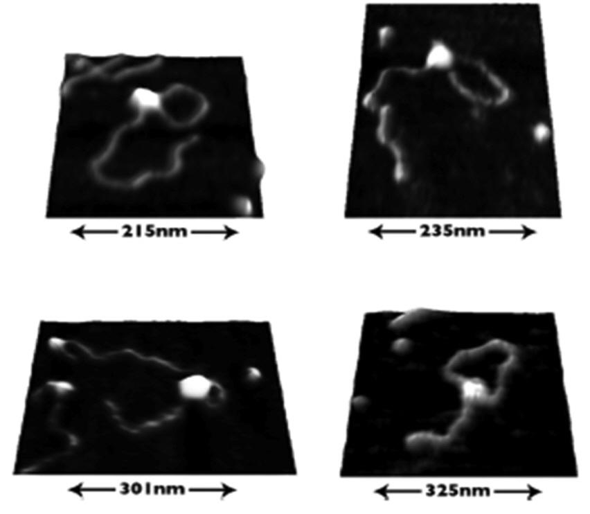
SECM and AFM were both developed as scanning probe microscopic techniques in the late 1980s. Since the invention and introduction of AFM in 1986 [13], AFM has been widely used to investigate the surface of polymers [24,25] and bio-materials [26] in singlestrain molecules with high resolution [27] and on the atomic scale [28]. For example, AFM has been employed to investigate single protein-DNA interactions (Fig. 1) [29]. Briefly, for AFM measurements, an ultra-small (a few nanometers) probe tip is positioned on a vibrating cantilever and the tip produces electrical or mechanical signals as it interacts with the sample surface. The movement and position of the cantilever are optically monitored by a laser beam and photodetector while the tip scans the sample surface. The atomic force between the tip and the material surface causes bending of the cantilever when the tip moves close to the surface. For example, electrostatic repulsion and attraction between the tip and substrate, or mechanical tip-substrate contact at surfaces with different degrees of stiffness and elasticity, result in different amounts of bending of the cantilever; the surface properties of the sample are then characterized in the AFM images based on the degree of bending of the cantilever [23].
SECM was invented by Professor Allen Bard in 1989 to study all types of surfaces in gases and solutions using electrochemical measurements (Fig. 2) [30]. SECM employs an ultramicroelectrode (UME, an electrode with a diameter of less than 100 μm), a bipotentiostat, and an XYZ positioner to study the surface using electrochemical signals detected by the UME tip. In electrochemistry, the changes in the current over an experimental timeframe at certain applied potentials depend on several factors such as the shape and size of the electrodes, the reactant concentration at the electrode surface, the electron transfer rates or reaction kinetics at the electrode, and mass and ion transfer in the bulk solution. When the distance between the electrode probe and insulating substrate decreases on the dimensional scale of the tip diameter or diffusion layer thickness (a few tens of micrometers), the current measured at the UME is reduced because mass transport of the reactants to the electrode is hindered by the small distance between the electrode and the substrate [30,31]. The currentdistance behavior at the insulating surface is termed the negative feedback mode of SECM (Fig. 3) [31]. In contrast, when the UME approaches a conducting substrate, the reduced or oxidized species at the tip electrode are regenerated at the conducting substrate, thereby furnishing more reactants to the UME probe. Consequently, the measured current increases exponentially as the distance between the UME and the substrate decreases as the diffusion length and time required for shuttling the reactants between the UME and conducting substrate is reduced. The increase in the current with decreasing distance is termed the positive feedback mode of SECM (Fig. 3). By interpreting the diffusion-limited current measured at the UME, SECM can provide information on the electrochemical properties of insulators, semiconductors, conducting surfaces, and bio-films [32-34]. Examples of SECM studies aimed at developing catalytic materials are provided below.
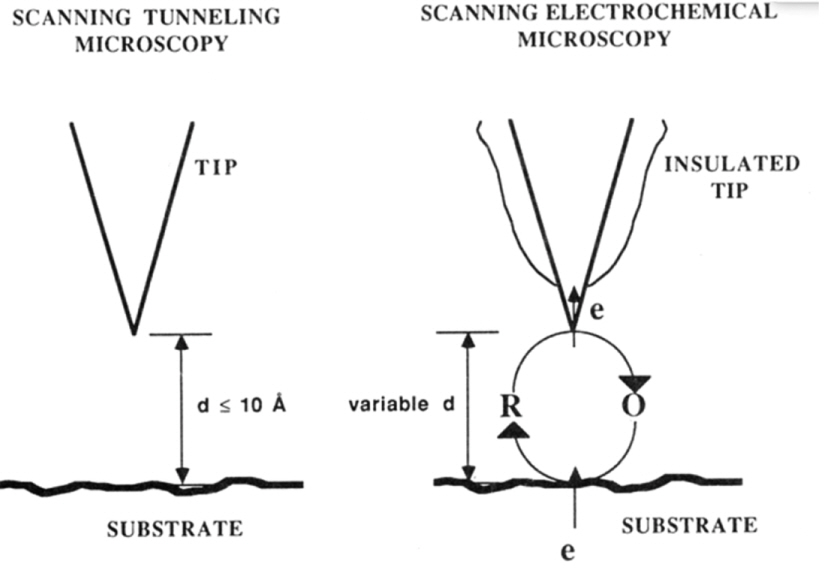
Schematic displaying principles of scanning tunneling microscopy (STM, left) and scanning electrochemical microscopy (SECM, right); d is the spacing between the tip and the substrate, and R and O represent the reductant and oxidant, respectively. “Tip” is the conducting electrode with dimensions of a few tens of micrometers. Reprinted with permission from Ref. [30]. Copyright [1989], ACS publications.

Normalized current-normalized distance curve obtained using positive (circle) and negative (triangle) feedback mode of SECM; iT is the tip current with a specific normalized distance; iT,infinite is the current measured when the tip is placed in the bulk solution at a large distance from the substrate; d is the spacing between the tip and substrate; and a is the radius of the UME. Reprinted with permission from Ref. [31]. Copyright [2011], RSC publications.
3. Electrode Development for SECM
Many electrocatalytic reactions, i.e., complex inner-sphere electrochemical reactions with multielectron transfer, occurring at the surface of electrocatalysts have been studied using SECM techniques. Hydrogen evolution or hydrogen oxidation reactions (HERs/HORs) at the surfaces of Pt, Au, and other metals were investigated using the positive or negative feedback mode of SECM, discussed above [31,35,36]. In order to verify the activity of the electrocatalysts using SECM, the probe UME tip should be placed close to the sample substrate with a distance less than the tip diameter and i) the electrochemical species produced at the substrate are detected at the UME tip, i.e., tip-collection and substrate-generation (TC/SG) mode of SECM, or ii) the reactants required for the electrocatalytic reaction at the substrate are generated at the UME tip, i.e., tip-generation and substrate-collection (TG/SC) mode of SECM (Fig. 4) [35]. As the probe UME scans the surface of the substrates at micrometer resolution, quantitative assessment of the activity of the unidentified electrocatalysts using SECM in the TC/SG or TG/SC mode is possible, provided that the collection efficiency of the TC/SG (or TG/SC) method is known, i.e., the ratio of collected chemicals reacted at the tip (or substrate) with the generated reactant at the substrate (or tip). The collection efficiency at particular tip-substrate positions should be measured separately using redox couples with fast reaction kinetics, e.g., Fe(CN)62+/3+, Ru(NH)62+/3+, or ferrocene0/+, where the reactions do not require catalytically active surfaces. The faradaic efficiency or activity of the catalysts can be calculated by comparing the measured current at the tip (or substrate) with the theoretical current by considering the collection efficiency.

Current-potential curves generated using SECM in substrate generation/tip collection (SG/TC) mode. Oxidation of ferrocene-methanol at the substrate and reduction of ferrocenium-methanol were measured in 1 mM ferrocene-methanol and 0.1 M K2SO4 aqueous solution. The substrate potential was scanned from 0.3 to 0.7 V (vs. RHE) at a scan rate of 2 mV s−1, and the tip potential was held at 0.3 V. The distance between the tip and substrate was controlled at 5 (black), 10 (red), 15 (blue), and 25 μm (green). Tip radius was 25 μm. Reprinted with permission from Ref. [35]. Copyright [2008], ACS publications.
Bard and coworkers used SECM to screen active electrocatalysts for water splitting on conducting [37] or semiconducting electrodes for electrocatalytic and PEC reactions [12]. For example, PEC water splitting reactions were studied by using SECM with n-type metal oxide electrodes (such as BiVO4) coated with OER catalysts. IrO2 and CoOx films are considered among the best OER electrocatalysts for use in aqueous solutions. However, most studies on electrocatalysis using OER catalysts have been performed with electrocatalyst films coated on conducting substrates [10]. For example, IrO2 and CoOx films layered on fluorine-doped tin oxide (FTO) presented overpotentials of approximately 200 and 100 mV; these were less than that obtained with a Pt electrode at 0.5 mA cm−2 for the OER in a neutral phosphate buffered aqueous solution [12]. Ye et al. applied IrO2, CoOx, and Pt spot-arrays on semiconducting electrodes to PEC OER reactions under UV-vis irradiation, where the arrays were formed by dispensing pico-liters of precursor solutions on n-type metal oxide semiconductors [12]. The activity of the different OER catalysts was investigated under photo-illumination using SECM configurations. The SECM experiments demonstrated that Pt on W-doped BiVO4 was the most active catalyst, whereas IrO2 and CoOx on the semiconducting electrodes were not as active as the same species on the conducting substrate. The different results obtained for the catalysts on conducting and semiconducting electrodes imply that the electrocatalyst and substrate interactions may be significantly important for catalytic reactions because electron transfer through the electrode-catalyst interface greatly influences the overall activity. In the aforementioned study, a comparison between different OER catalysts was possible by employing SECM in rapid screening experiments under various conditions.
The faradaic efficiency is an important parameter that indicates the stability and selectivity of catalysts for the intended electrochemical reactions. The faradaic efficiency is the ratio of the current used for the reaction of interest to the total current measured during the process. If non-faradaic reactions such as double-layer charging or side-reactions (e.g., electrode decomposition or unintended reactions at the electrode) occur, the faradaic efficiency is below 100%. The faradaic efficiency of a cobalt OER catalyst decorated on metal nitride and metal oxide electrodes was also determined using SECM in the TC/SG-mode [28,29]. Cong et al. utilized a gold ring-fiber disk electrode to irradiate a substrate, i.e. catalyst-semiconductor electrode, with UV-vis light, while the gold ring electrode titrated the oxygen generated at the substrates. The diameter of the optical fiber core was 200 μm and the thickness of the gold ring coated around the fiber was 20 μm. To precisely detect the oxygen generated on the substrate, the distance between the substrate and probe electrodes was controlled to approximately 60-80 μm using the XYZ positioner, which resulted in a theoretical collection efficiency approaching 68%. The effects of the cobalt electrocatalyst were clearly demonstrated in the SECM experiments, and the faradaic efficiency of the catalyst coated Ta3N5 nanotube was approximately 80-90%; however, almost no oxygen was detected without the use of an electrocatalyst [28,29]. The results indicate that the excited minority carriers of n-type metal nitrides generated by the absorbed photons decomposed the electrodes themselves due to the slow OER kinetics in the absence of OER catalysts; the decomposition reactions were effectively mitigated by facilitating transfer of the charge to water oxidation via cobalt electrocatalysts.
Efficient semiconducting photocatalysts for water oxidation were also developed by rapid screening methods using SECM [40-43]. The semiconducting properties, e.g., the size of the band-gap, doping densities, carrier lifetime, and rates of charge recombination and transport, are strongly interrelated and are significantly affected by the composition and crystal structure of the semiconductor materials. SECM was used for facile preparation and characterization of n-type metal oxides such as BiVO4, Cu-In-Bi oxides, Zn-In oxides, W-Cd oxides, and chalcogenides (e.g., WSe2 or CdSe) [40-43]. For example, the optimum dopant composition for the metal oxide photocatalyst, BiVO4, for photo-oxidation reactions was determined using SECM techniques after screening more than 500 different catalyst compositions with various kinds of dopants (Fig. 5) [43].

Schematic diagram of the atomic composition of dispensed photoelectrocatalysts on FTO (a). Each spot has a total of 18 drops of the precursor solutions of Bi/V (0.1 or 0.02 M), W (0.02 M), and Mo (0.02 M) prepared in ethylene glycol. Photoactivity of spot arrays was measured at 0.4 V vs. NHE in 0.1 M Na2SO3 and 0.1 M Na2SO4 solution under UV-visible irradiation (b). Reprinted with permission from Ref. [43]. Copyright [2011], ACS publications.
In addition to the functional aspect of the SECM study described above, fundamental aspects of catalytic reactions were investigated using SECM. For example, SECM was used to detect reactive radicals adsorbed on the electrode surface to deepen the understanding of the physicochemical mechanisms of the water oxidation reactions [44,45]. Zigah et al. and Park et al. evaluated the density of hydroxyl radicals adsorbed on the surfaces of TiO2 and BiVO4 electrodes and the rate of dimerization of the hydroxyl radicals (reaction 3), where the radicals were produced as a reaction intermediate of the OER [44,45].
2OH·(adsorbed) → H2O2 (k = 4 × 10³ mol−1 m2 s−1, reaction 3)
Briefly, the metal oxide semiconductor was placed in an aqueous solution in the traditional three-electrode configuration. A Ag UME with a diameter of 50 μm was then placed on the metal oxide electrode at a controlled distance (e.g., approximately 12 μm) between the UME and metal oxide film. The electrochemical information was finally measured using SECM in the transient positive/negative feedback mode, also called the surface-interrogation mode of SECM (SI-SECM). In SI-SECM, the adsorbed species generated at the substrate (SG) are titrated using the chemical produced at the tip (TG). The limited tip current is measured until the titration is completed and all adsorbates are consumed. The decay kinetics and the densities of the surface adsorbates are measured by quantifying the collected tip current and titration time in SI-SECM. In SI-SECM, the theoretical collection efficiency of SECM should be considered to analyze the measured current at the tip electrode, and the accuracy and detection limit of the measurement are determined by the size of the tip electrodes and the distance between the two electrodes.
4. SECM with Nanometer Resolution and AFM-SECM
When a conventional UME with a diameter of tens of micrometers is used for SECM, the activity measured from the electrodes coated with nanoparticle electrocatalysts must be averaged over a number of particles on the electrode so that the obtained result is still an ensemble average value rather than the value for a single nanoparticle, as presented above. In order to tackle the electrochemical problems in single nanoparticle regimes, SECM analysis on the submicrometer scale is required [46-50]. For example, Fig. 6 shows scanned images from SECM experiments employing a nano-sized electrode with a diameter of 160 nm [51]. During the measurements, the small tip approached the disk substrate at a constant vertical distance of 5 μm; the electrochemical activity and topology of the substrate were then assessed by scanning using Ru(NH3)62+/3+ as a redox couple. In addition, topological images of the bio-cells were obtained at micrometer resolution using an ~1 μm carbon disk electrode (Fig. 7), where the substrate exhibited no electrochemical activity [52].
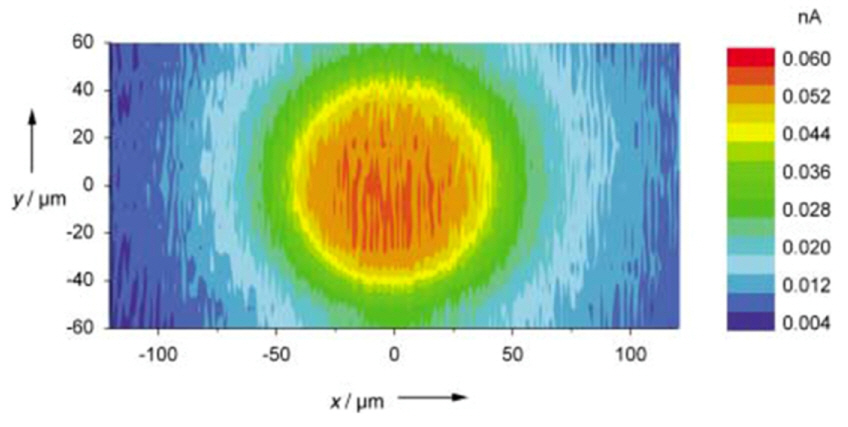
SECM image of disk electrode (r = 40 μm) using nano-size probe (r = 80 nm). Tip-substrate distance was 5 μm and SECM was used in TC/SG mode employing a Ru(NH3)62+/3+ redox couple in 5 mM Ru(NH3)6Cl3 and 0.1 M KF aqueous solution. Reprinted with permission from Ref. [51]. Copyright [2004], Wiley-VCH Verlag GmbH & Co.
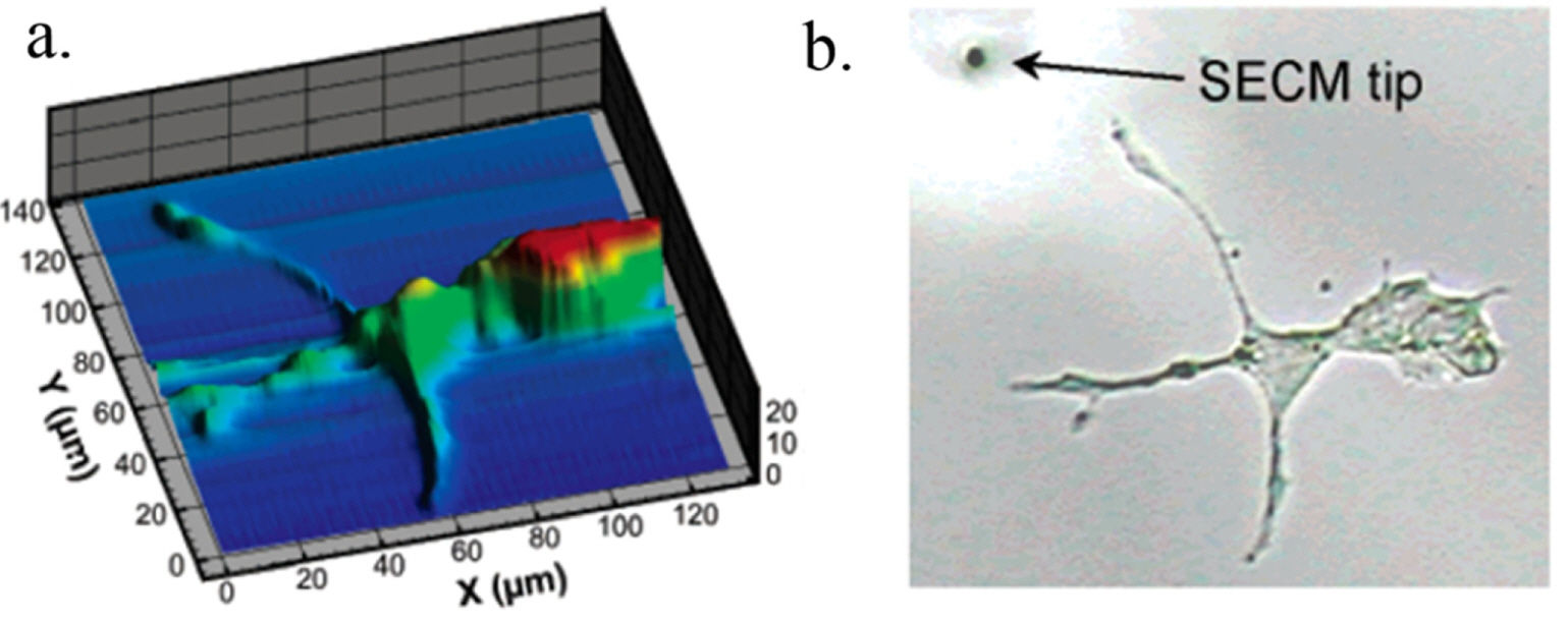
PC12 cell imaged via SECM using ~1 μm diameter carbon disk electrode (a) and optical microscope image acquired during SECM experiments (b). 1 mM Ru(NH3)62+/3+ redox couple in aqueous solution was employed in the SECM measurement in negative feedback mode. Reprinted with permission from Ref. [52]. Copyright [2005], ACS publications.
By using small UMEs, the electrochemical activity of a single nanoparticle has also been measured for hydrazine oxidation on Pt and for the OER over IrOx nanoparticles by conducting simple chronoamperometry [53,54]. Measurement of the activity of a single nanoparticle in catalytic reactions was based on diffusion-controlled stochastic collision, where the nanoparticles were dispersed in an electrolyte solution and collided with the surface of the UME. Stepwise variation of the measured current at the UME indicates occurrence of catalytic reactions on single nanoparticles in each collision event. Thus, the activities of individual nanoparticles could be separately observed. However, this approach is not suitable for the analysis of electrode-supported catalysts when no stochastic events are expected.
To truly understand electrocatalysis using supported electrocatalysts at the single nanoparticle level, a smaller probe electrode with dimensions of a few tens of nanometers and new SECM techniques are required, as stated above. The nano-SECM measurement also allows for evaluation of the interactions between single nanoparticles and larger substrates and their specific catalytic activity for catalytic reactions, e.g., the HER and OER. As previously explained, the spatial and temporal resolution of SECM measurements are limited by the size of the probe tip electrode, i.e., the UME, where the measured signal is the diffusion-limited faradaic current detected by the probe electrodes [40]. A UME with a diameter larger than 10 μm is commercially available, and UMEs with diameters of a few micrometers, prepared in-house, have often been employed in laboratory analyses. In order to study single nanoparticles, including small enzymes and even molecules, significant effort has been devoted to fabricating electrode tips in the nanometer size range, having a controlled shape and defined active area [50]. As shown in Figs. 6 and 7, a nanometer-sized electrode has been used in SECM, though the measurement was performed on a large biological sample with a length scale of a few tens of micrometers [51]. Scanning nanometer-sized samples such as single nanoparticles or single enzymes remains a challenge, even though the electrochemical activity of such species should be monitored to fully understand the catalyst properties, as described in the previous section.
In order to achieve nanometer resolution in SECM analyses, the AFM technique was recently combined with SECM. Thus, the combined AFM-SECM technique using an AFM cantilever with a conductive coating as the tip electrode for SECM has led to recent progress [55-63]. A number of approaches have been attempted in order to use the conductive cantilever as the tip electrode, with the objective to confine the active tip area of the AFM cantilever. For example, chemical probe molecules were attached to the apex of the tip or to nanoparticles on the substrate to shuttle the electrons between the tip electrode and substrate for the electrochemical reactions (Fig. 8a) [58]. However, this chemical modification method is unsuitable for the evaluation of catalytic reactions using SECM where the chemical probe molecules cannot be used. A tip fabricated with a defined exposed area similar to the conventional UME is more suitable for various electrochemical techniques developed for SECM.
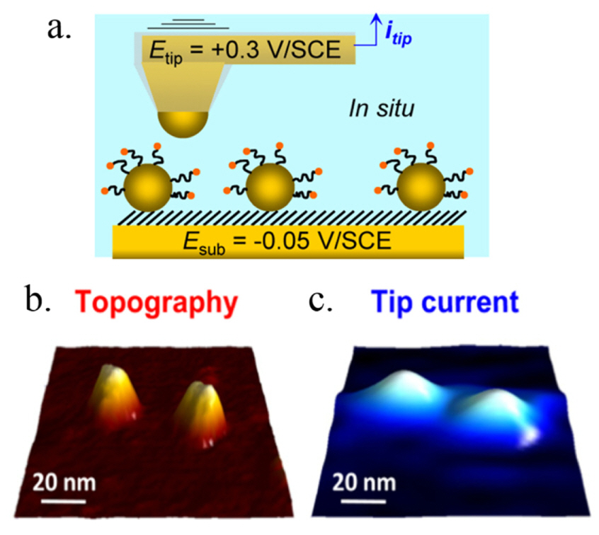
Schematic diagram of AFM tip scanning of ferrocene-PEGylated gold nanoparticles in SECM mode (a). Simultaneous observation of single gold nanoparticles in AFM (b) and AFM-SECM (c) mode using AFM probe electrode. The electrochemical signal was measured from the oxidation reaction of chemical probes, i.e., ferrocene-PEGs attached on the gold nanoparticle surface, at the AFM tip and the oxidized chemical probes were again reduced at the gold nanoparticle surface. Reprinted with permission from Ref. [58]. Copyright [2013], ACS publications.
In order to construct tip electrodes to broaden the application of AFM-SECM to a scope similar to that of the UME, tip electrodes have been prepared via mechanical (or chemical) insulation of the conductive cantilever [56,57]. In these methods, most of the conducting area of the cantilever was covered by employing various techniques, e.g., physical insulation by polymer films or electrophoretic deposition of chemicals, followed by mechanical abrasion or electric discharge methods to expose the end of the tip as the active electrode [56,57,59,60]. For example, electropaint concentrated in an organic solvent (Clearclad HSR, Harvey, IL) was used to cover most of the conducting area of the AFM cantilever by an electrochemical anodic/cathodic deposition method [59]. Prior to electrodeposition of the electropaint on the cantilever, the electrical contact should be prepared on the body of the cantilever to connect the conducting cantilever to the potentiostat. The electrodeposited organic molecules on the cantilever produce resistive films that eventually prevent further electrodeposition. The insulating films deposited on the cantilever are then cured at high temperature. After annealing, the insulator/tip composite is positioned in the AFM for interaction with the sample surface. The insulating film at the tip apex can be removed using the contact mode of AFM; mechanical abrasion during the AFM scan exposes a small area of the conducting tip. Finally, the tip cantilever with the exposed conducting apex is ready to be used for electrochemical measurements in the AFM configurations. The exposed conducting area, which quantitatively defines the active electrode area, is of the order of nanometers, and various SECM techniques can now be used with a resolution of several nanometers under severely oxidative and reductive reaction conditions using the robust tip electrode (see below).
Since the combination of AFM-SECM was first introduced [55], intensive effort has been expended to increase the resolution of the measurements and to develop practical methods for tip preparation. Figs. 8b and c show recent reports in which single nanoparticles (20 nm) were analyzed using the AFM and AFM-SECM techniques [58]. A homemade AFM tip electrode with a diameter of approximately 200 nm was fabricated by melting a gold micro-wire using electric arc heating. Nanoparticles placed on the substrate electrode were surface-modified with ferrocene-polyethylene glycol to facilitate electrochemical detection using the AFM probe. The ferrocene molecules were tethered to the nanoparticle to shuttle electrons between the nanoparticle and the tip, resulting in a flow of current. However, the molecule-mediated SECM-AFM scanning method cannot be used to study various catalytic reactions where no redox mediator is present. Abbou et al. reported approach curves of AFM-SECM using a gold AFM-tip electrode with spherical geometry (radius of 155 nm) fabricated by electrophoretic coating [57] (Fig. 9a). The approach curve obtained in the positive feedback mode of AFM-SECM was in agreement with the expected simulations in the sub-micrometer regimes (Fig. 9b and c). The cyclic voltammograms (CVs) acquired with the AFM-tip electrode were also well explained by the simulated CV using a spherical electrode with a radius of 155 nm. Derylo et al. demonstrated more practical applications of AFM-SECM, where the AFM-tip electrode was prepared by the electrodeposition of parylene, followed by mechanical abrasion to expose the end of the tip (diameter less than 200 nm) [56] (Fig. 10). The AFM-tip was then engaged to obtain electrochemical images of the porous poly(imide) membranes using SECM in the TC/SG-mode. The imide film contained micrometer-sized pores though which Ru(NH6)3+ diffused out and was reduced at the AFM-tip electrode (Fig. 10). The electrochemically scanned image obtained from the AFM-SECM measurements was also well supported by the topographical images obtained from the AFM experiments.

Scanning electron microscopy image of sub-micrometer AFM-tip electrode (a). AFM approaching curve (b) and AFM-SECM approaching curve (c) obtained using the AFM-tip electrode in 1 mM ferrocene-methanol and 0.1 M KH2PO4 aqueous solution. Reprinted with permission from Ref. [57]. Copyright [2002], ACS publications.
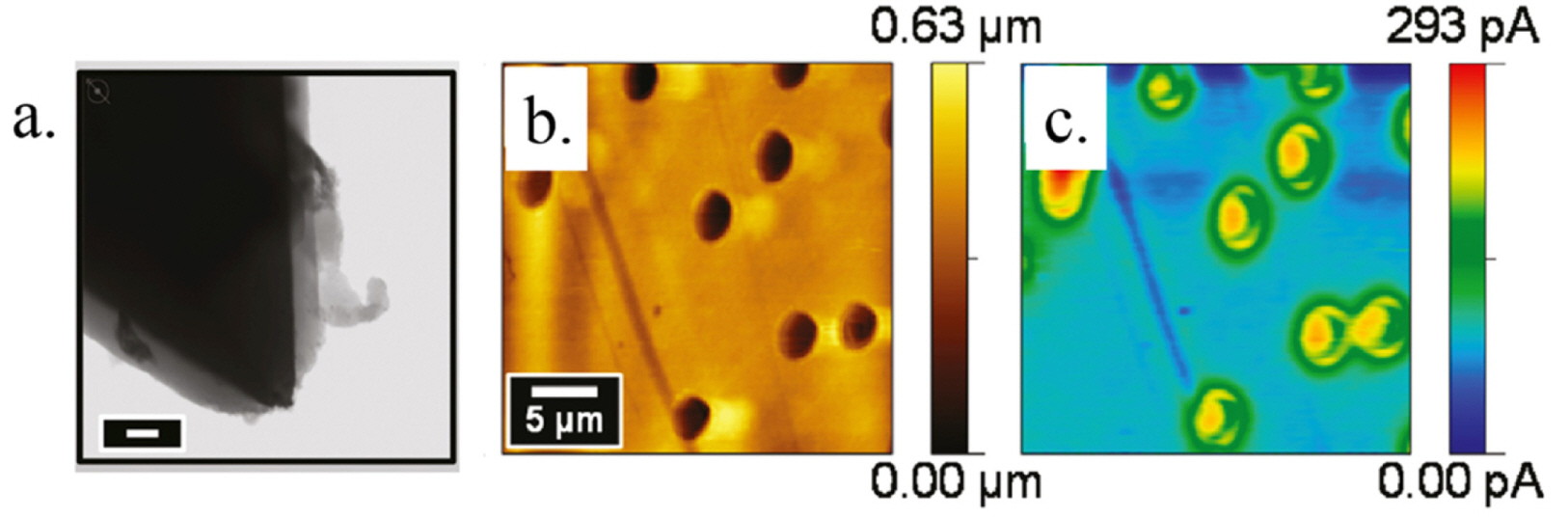
Scanning transmission electron microscopy image of sub-micrometer conductive AFM-tip electrode coated with parylene (a). Scale bar represents 200 nm in (a). The coated tip end was exposed by mechanical abrasion during AFM operation. Topographical image of a porous poly(imide) film, acquired via AFM in contact mode (b) and AFM-SECM image of the identical film using the reduction of Ru(NH)63+ that diffused through the pores; detected by the AFM-tip electrode (c). Reprinted with permission from Ref. [56]. Copyright [2011], ACS publications.
5. Outlook
As discussed in this mini-review, AFM-SECM can be applied to study the electrochemical properties of single nanoparticles, and can further be used to study the effect of the catalyst/substrate interface (or that of the substrate electrodes) on the catalytic activity of individual nanoparticles in complex electrocatalytic reactions. Several methods have been used to insulate the AFM cantilever (except for the very end of the tip), such as electrodeposition of electrophoretic paints, mechanical abrasion, electrical arc discharging, and chemical modification. However, the application of AFM-SECM techniques is still limited to preliminary studies, and the practical application of AFM-SECM has not been widely demonstrated, mainly due to the difficulties associated with electrode fabrication.
The essential areas for future development of AFM-SECM and for further contribution to the existing technologies can be summarized as: (i) the development of facile approaches for the preparation of electrochemical probes with a defined conductive tip area, exposed on the nanometer scale and (ii) practical application of SECM techniques, such as positive/negative feedback, redox competition, surface interrogation, tip generation/substrate collection, or the substrate generation/tip collection mode to AFM-SECM to facilitate study of various electrochemical reactions with nano-meter spatial resolution. If AFM-SECM techniques using the practical probe electrode can be successfully implemented, the advanced knowledge obtained from AFM-SECM should accelerate progress in the field of electrocatalysis with deeper understanding of catalysts and electrodes at nanometer resolution.
Acknowledgements
This work was supported by the Korean Government through the New & Renewable Energy Core Technology Program of the Korea Institute of Energy Technology Evaluation and Planning (KETEP) funded by MOTIE (No.20133030011320 and No. 20153010041750) and the National Research Foundation of Korea funded by the MSIP (NRF-2015M1A2A2056554). This study was also financially supported by the KIST through the Institutional Project.