Development of Macro-Porous Silicon Based Dye-Sensitized Solar Cells with Improved Light Trapping
Article information
Abstract
The light harvesting efficiency is counted as an important factor in the power conversion efficiency of DSSCs. There are two measures to improve this parameter, including enhancing the dye-loading capacity and increasing the light trapping in the photoanode structure. In this paper, these tasks are addressed by introducing a macro-porous silicon (PSi) substrate as photoanode. The effects of the novel photoanode structure on the DSSC performance have been investigated by using energy dispersive X-ray spectroscopy, photocurrent-voltage, UV-visible spectroscopy, reflectance spectroscopy, and electrochemical impedance spectroscopy measurements. The results indicated that bigger porosity percentage of the PSi structure improved the both anti-reflective/light-trapping and dye-loading capacity properties. PSi based DSSCs own higher power conversion efficiency due to its remarkable higher photocurrent, open circuit voltage, and fill factor. Percent porosity of 64%, PSi(III), resulted in nearly 50 percent increment in power conversion efficiency compared with conventional DSSC. This paper showed that PSi can be a good candidate for the improvement of light harvesting efficiency in DSSCs. Furthermore, this study can be considered a valuable reference for more investigations in the design of multifunctional devices which will profit from integrated on-chip solar power.
1. Introduction
The light-harvesting efficiency (LHE) is one of the key features for high performance photovoltaic devices. This feature is derogated by reducing film thickness in thin-film solar cells such as dye sensitized solar cell (DSSC); therefore, many approaches are made to improve it. For example, porous active layer with high surface area [1-3], hierarchically nanostructures as photoanode [4-6], scattering layers on the top of active film [7-9], plasmonic photoanodes [10-12] and photonic crystal photoanodes [13-15] have been applied for changing the optical design of the DSSC to optimize its light absorbance. Since the mentioned approaches have some limitations like high reflectance loss and low dye adsorption, researchers are still extensively eager to explore the new light trapping structures as photoanode.
Surface texturing is one of the most powerful techniques to improve thin film solar cell's efficiency. These textured substrates increase the LHE by: (a) reducing the probability of optical reflection of the front surface, (b) lengthening the optical path of the light through the cell, (c) trapping a greater percentage of light within the thin active layers, and (d) increasing the electrode's surface area [16-18]. In the recent years some publications have reported the employing of surface textured substrates as photoanode for DSSCs, too.
Reports of employing textured glass, patterned FTO, textured-3D TiO2 active layer, and alternative grooved substrates like Ti metal as photoanode have resulted a significant increase in conversion efficiency. Hussain et al. reported the ICP-RIE textured glass substrate as photoanode. Their textured glass substrate showed the high diffused transmittance and haze ratio in the visible-NIR wavelength region, which was suitable for high performance DSSCs [19]. Also, maskless RIE pre-textured glass substrates as photoanode has been introduced to DSSC by Chen et al. [20]. Another notable enhancement in power conversion efficiency was achieved through the reduction in reflections of the visible range and increasing effective cell interface area. In a study by Kong et al. a DSSC fabricated on the patterned FTO electrode and the effect of surface modification was investigated [21]. That cell showed higher photocurrent using larger surface area of the patterned FTO which allows more involvement of TiO2 particles and dyes. In 2013, Wooh et al. demonstrated a light-trapping strategy in DSCs with textured and 3D photoanodes made from TiO2 nanoparticles [22]. The novel structure showed higher light absorbance and hence higher photocurrent in comparison with the ordinary 2D flat photoanode. It is noticed that better performance was due to the increase of the light path length caused by the reflection of the scattered light on the tilted facets of the textured structures. Also, Nath et al. introduced hierarchically arranged light-scattering layers (LSLs) into the regular TiO2 films of DSSCs to enhance the LHE in the visible region of light [23]. The optical density was significantly enhanced inside the film by the effect of producing higher wavelength light gradually with an increase in scattering particle size. The power conversion efficiency of the cells with scattering layers was enhanced up to 32% for wavelengths ranging from 550 to 800 nm compared with cells without scattering layers. In another research a thin TiO2 underlayer with a grooved structure was prepared on a Ti metal [24]. This textured underlayer decreased the charge transfer resistance at the Ti metal/ TiO2 interface and importantly improved the light harvesting ability of the cell.
This research looked into the possibility of having light trapping process in DSSC by using macroporous silicon (PSi) substrate as photoanode. To the best of our knowledge, this is the first work that shows how the DSSC's performance parameters, such as short-circuit current density, open circuit voltage, fill factor, and power conversion efficiency affected by the geometric properties of porous silicon. Three different PSi samples were formed using electrochemical anodization. Afterward ITO film was deposited on PSi substrates with DC magnetron sputtering, which was followed by the subsequent deposition of a TiO2 layer by using sol-gel spin-coating. Finally, the proposed DSSCs have been assembled. An investigation including energy dispersive X-ray spectroscopy, photocurrent-voltage, UV–visible spectroscopy, reflectance spectroscopy, and electrochemical impedance spectroscopy measurements has been carried out in order to characterize the suggested DSSC. PSi substrates with different textured surface changed both the optical property and dyeloading capacity which ameliorate light harvesting efficiency far better.
2. Experimental Section
2.1 Preparation of Macro-Porous Silicon
Many physical and chemical methods have been proposed for texturing of silicon surface, such as mechanical grooving [25], lithography followed by reactive ion etching [26], laser texturing [27], and electrochemical etching. Porous silicon prepared by electrochemical etching is of interest due to the ability for fabricating various structures and cost effectiveness [28,29].
In our experiments, (1 1 1) and (1 0 0)-oriented n-type, Czochralski-grown, single crystal Si wafers with thickness of 430 ± 20 μm and resistivity of 1.5 ± 0.2 Ω cm used as starting materials. The wafers were first cut into 1.5 × 1.5 cm2 square samples and then samples were dipped in 1:10 dilute HF solution to remove all traces of native oxide. Before etching procedure, samples were chemically cleaned by standard RCA procedures and dried under a stream of N2 gas respectively. The PSi was prepared by electrochemical anodization method in an electrolyte of 40 % hydrofluoric acid, DI water, and 99.9 % ethanol [HF: H2O:C2H5OH]. Ethanol is often added to the HF solution to reduce its surface tension. The Si sample and Pt disc were connected as anode and cathode respectively. Approximately 0.25 cm2 of the polished side of the Si sample was exposed to the etching solution. PSi formed by this method can present various shape and size, depending on formation parameters including current density, electrolyte concentration, and etching time. By optimizing the etching conditions, PSi samples with the pore diameter in micrometer scale were prepared. After chemical etching, the surface-processed Si was rinsed several times in ethanol and dried [30].
2.2 Preparation of TiO2 Sol
The sol-gel procedure with a titanium-alkoxide sol was used for synthesis of TiO2 sol. Titanium tetra isopropoxide (TTIP, 97%, Sigma-Aldrich) was used as titania precursor and ethanol, nitric acid (HNO3) and de-ionized water were used as received. First, the titanium tetra isopropoxide was mixed with ethanol, and the de-ionized water was added drop wise under constant stirring for 1 h. Then, the resultant solution was peptized using (0.1 mol) nitric acid, to maintain the pH of the solution, and refluxed at 80 ℃ for 8 h. Finally, a white and highly viscous solution was obtained [31-33].
2.3 Preparation of Photoanodes and DSSCs
The prepared nanoparticle TiO2 sole was coated onto ITO-coated PSi substrates by spin-coating technique. This process was controlled by multiple spin-coating and drying steps. The thickness of TiO2 films above the PSi substrates’ surface was about 2 μm with good filling in the micro-pores. After drying in air the TiO2 photoanodes were heated at 100 ℃ for 15 min which was followed by sintering at 400 ℃ for 30 min. The resulted photoanodes, after cooling down to 120C, were immersed into a solution of N719 dye in ethanol for 24 h at room temperature for complete dye adsorption. Afterwards, the photoanodes were rinsed with anhydrous ethanol to wash redundant dye molecules away. Counter electrodes were prepared by spin-coating 4 wt% H2PtCl6 solution onto the ITO glass and heating at 450 ℃ for 30 min. The dye-adsorbed TiO2 photoanodes and the Pt-coated counter electrodes were assembled into a sandwich-type cell using a clamp and sealed with a hot-melt sealant of 80 μm thick. The electrolyte solution was a mixture of LiI (0.5 M), I2 (0.05 M), and 4-tert-butylpyridine (0.5 M) in acetonitrile and was injected through a drilled hole in the counter electrodes. In the next step the hole was sealed using a cover glass. The final active area of the cells was 0.25 cm2 [33]. In this work, traditional ITO glass-based photoanode was also fabricated with the same process. The thickness of TiO2 film was about 15 μm.
2.4 Characterization
In this study, porosity of the PSi samples was measured by gravimetric method. Percent porosity is defined as the fraction of voids inside the porous layer verses the starting silicon. This parameter is calculated by gravimetric technique. The original crystalline silicon sample is weighed first (m1), then PSi is formed and the sample is weighed again (m2), finally the PSi layer is removed and the sample is weighed once more (m3). The selective removal of the porous Si layer-with no effect on the bulk crystalline silicon-is made by dipping for a few minutes in an aqueous solution of KOH (3% in volume). With these three measurements, determination of the percent porosity was possible by [30]:

The microstructure and surface morphology of the PSi samples were investigated by a Hitachi S-4800 scanning electron microscope (SEM) with Energy Dispersive X-Ray (EDX) detector. The presence of deposited layers on PSi samples was confirmed by EDX analysis. The crystalline nature and the phases of the TiO2 coated PSi samples were studied by a Philips X’Pert MPD X-ray diffraction (XRD) instrument with CuKα of 1.540 56 Å. Photovoltaic measurements employed an AM 1.5 solar simulator (Luzchem Research) at 25 ℃ equipped with an Autolab PGSTAT302 N potentiostat/galvanostat. The power of the simulated white light was calibrated to 100 mW/cm2. Electrochemical impedance spectra (EIS) measurements were taken over a frequency range of 0.1 Hz-100 kHz with 10 mV amplitude at open-circuit conditions under standard global AM 1.5 solar irradiation. Reflectance of the obtained PSi samples was evaluated by reflectance spectroscopy measurements using an avantes spectrometer (Avaspec-2048-TEC). The amount of dye was determined by desorbing the attached dye molecules of the substrates in 0.1 M NaOH aqueous solution, with the concentration measured by a UV-Visible spectrophotometer (Perkin Elmer, Lambda 25).
3. Results and Discussion
3.1 Microstructural Characterizations
Porosity level, geometry, and microstructure of pores depend on the anodization conditions. These conditions include electrolyte concentration, etching current density, etching time, silicon wafer characteristic, illumination (required for n-type silicon), and temperature. Table 1 summarizes the experimental conditions of the three PSi samples which prepared in this investigation. In order to yield a better wetting properties of the Si surface, the compositions of the etch solution was (HF: Ethanol: DI) = (25 %: 60 %: 15 %). Also the etch temperature was 40 ℃ and all samples were made porous electrochemically by constant 24 mA/cm2 current density when exposed to the white light. Fig. 1 shows the SEM images of three PSi samples fabricated using the proposed electrochemical anodization method at the different etching conditions. For PSi(I), the V-shaped structure at the bottom of the pores and hexagonal shape at the surface is because of (111) wafer orientation. Cross-sectional SEM images clearly demonstrate the pores size (diameter on top) in the range of 3-4 μm and their depth about 5 μm. For PSi(II) and PSi(III), the curveshaped structure at the bottom of the pores and circular shape at the surface is an outcome from the (100) wafer crystal orientation. Top-viewed SEM images (Fig. 1f, i) revealed that for both of these samples the pores diameter is the same and equals to 3 µm. The increase of the pores depth by growing the etching time is clearly visible in the cross-sectional images (Fig. 1e, h). For PSi(II) with 15 min time etching, the macro-pores length is about 10 µm, while it’s approximately 15 µm for PSi(III) which had 25 min time etching. Despite having the same etching condition, PSi(I) compared with PSi(III) has pores with less depth since the (111)-oriented planes slowly etch in the etching solution. The pore size, depth, and distribution are largely uniform and reproducible across the all three samples. Also, by Using gravimetrical technique the percent porosity values of 51 %, 53 % and 64 % is calculated for PSi(I), PSi(II) and PSi(III) respectively.

Experimental conditions of different PSi samples.
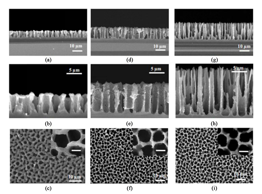
Cross-sectional and top view SEM images of the PSi samples fabricated using the proposed electrochemical anodization method at different etching conditions: (a,b,c) PSi(I), (e,f,g) PSi(II), and (h,i,j) PSi(III). Inset scale bars are 3 μm.
The ITO films with a thickness of 300 nm were deposited on PSi samples by DC magnetron sputtering technique, as described previously [34]. The electrical properties of the ITO films were determined by the four-point probe technique. The measured values demonstrate the sheet resistance of ITO/PSi structures in the range of 8-10 ohm/sq. As mentioned before, the TiO2 films prepared using sol-gel spin-coating method and annealed at 400℃. As an example, three steps of the TiO2 film deposition on PSi(II) by spin coating method are shown in Fig. 2a. Cross-sectional SEM images of the TiO2 film after 5 spin-coating times, 10 spin-coating times, and filling of the pores are respectively illustrated in Fig.2a-I, 2a-II, and 2a-III. Also High magnification SEM image of TiO2 film is shown in Fig. 2b. This image depicts nano-scale spherical particles of the film. The TiO2 grain size was observed to be about 30 nm. The formation of nano-sized smooth grains all over the surface can lead to improve the dye-loading capacity due to larger surface area. The crystal phase of TiO2 films was determined by X-ray measurements. As XRD pattern depicts the spin-coated TiO2 layer is largely in anatase phase (Fig. 3). This layer shows predominant anatase peaks at (101), (004), (112), (200), and (105). All peaks are in good agreement with the standard spectrum (JCPDS no.: 88-1175 and 84-1286). For dye-sensitized solar cells, anatase is perceived as the more active phase of TiO2 because of its surface chemistry and potentially higher conduction-band edge energy [35].
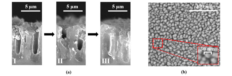
(a) SEM images of the TiO2 film deposited on PSi(II) by sol-gel spin coating method: I) 5 spin-coating times, II) 10 spin-coating times, III) after filling of the pores (b) High magnification SEM image of TiO2 film (inset: 30 nm TiO2 particle).
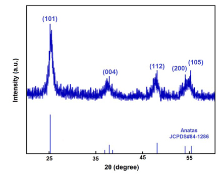
X-ray diffraction patterns of sol-gel spin-coated TiO2 films.
Elemental analyses of PSi samples based on Energy-dispersive X-ray spectroscopy (EDX) were also performed at various steps of the fabrication process (Fig. 4). A single peak at 1.74 Kev corresponding to Si was observed in the elemental analysis of Si wafer after electrochemical etching (Fig. 4(I)). The elemental analysis of ITO deposited on PSi sample (Fig. 4(II)) represents the presence of tin (Sn) and indium (In) distributed all over the porous substrate. Fig. 4(III) shows the EDX spectrum of sol-gel TiO2 film deposited on ITO coated PSi sample. The observed peaks at about 0.5, 4.5, and 4.95 KeV in this spectrum, which are assigned to O and Ti, demonstrate that this film is essentially pure.
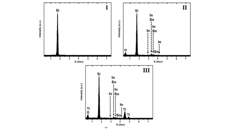
EDX spectrum of I) freshly prepared PSi sample, II) ITO deposited PSi sample, III) sol-gel spin-coated TiO2 film on ITO coated PSi sample.
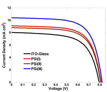
Current-voltage characteristics of DSSCs fabricated using different PSi samples.
3.2 DSSC performance of PSi-based photoanodes
Using the aforementioned samples as photoanode, three DSSCs were prepared and tested under 100 mW/cm2 sunlight. In order to evaluate the performance of these cells, a conventional ITO-glass photoanode with the same manufacturing process was made, too. Fig. 4 shows the photocurrent density versus potential curves of the cells. In addition, the resulting photovoltaic parameters derived from the J-V curves (Table 2). Power conversion efficiency values are 4.06%, 4.93%, 4.75% and 5.77% for photoanodes named as ITO-glass, PSi(I), PSi(II), and PSi(III), respectively. Comparing the photovoltaic performance parameters of the PSi-based DSSCs to the conventional DSSC, the PSi photoanodes in spite of the illumination through the counter-electrode are more photoactive than typical photoanode. Specially, the PSi(III)-based DSSC with deeper pores yielded a relatively large short-circuit photocurrent density JSC of 10.4 mAcm−2, which is higher than 8.03 mAcm−2 of the typical DSSC.
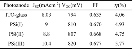
Photovoltaic performance of the DSSCs using various types of photoanodes.
It shows that the characteristics of macro-porous layer such as the size and depth of pores have a considerable impact on the efficiency. This improvement is attributed to the higher LHE of the novel photoanodes which is an effective factor for raising the JSC. This parameter is predominantly related to photoanode’s optical properties and dye-loading capacity.
UV-visible experiments were carried out to verify the influence of PSi structures on the amount of dye adsorption. We characterized the amount of dye adsorbed after detaching the dyes from four photoanodes with 0.1 M NaOH aqueous solution. The resultant UV-visible data are shown in Fig. 6. According to the spectra, the spectral line shapes have the same trends for all photoanodes. It is clear from this figure that light absorption is increased in PSi-based photoanodes in a wide spectral range of 400-700 nm compared to the conventional ITO glass-based photoanode. Among different PSi-based photoanodes, PSi(III) has the highest amount of dye-loading capacity. This increment is due to the high surface area to volume ratio of PSi, the percent porosity value of 64 %, which makes more surfaces available for TiO2. On the basis of this finding, we conclude that the presence of the PSi structures affects the dyeloading capacity considerably and thus they were found to have better photovoltaic performance than the conventional ITO-glass photoanode.

UV/vis absorption spectra representing the amount of dyes adsorbed in different photoanodes.
For investigating the possible light trapping effects, the diffuse reflectance of the prepared PSi samples was measured on a UV/Vis/NIR spectrophotometer. Fig. 7 shows the diffuse reflectance of the prepared PSi samples and polished single-crystal silicon wafer. It clearly shows that PSi structures drastically suppress light reflection over a wide spectral bandwidth. The average reflectance of the polished wafer, PSi(I), PSi(II) and PSi(III) in the wavelength range of 300-900 nm are about 35%, 5.7%, 7%, and 3.5% respectively. This remarkably low broadband reflectance indicates excellent light trapping ability of PSi structures which can be a major cause of improved photovoltaic performance of PSi-based DSSCs. Topographically rough, vertically aligned macro-porous structure may help to trap the light better and thus enhances the probability of photon absorption by the dye molecules. PSi(III) has significantly lower reflectance in comparison with two other samples that is due to deeper pores of this sample. Lower reflectance of PSi(I) compared to PSi(II), despite having shallower pores, can be an outcome from its pores’ shape. By comparing Table 2 and Fig. 6, it is concluded that there is a direct relationship between anti-reflective property and power conversion efficiency.

Reflectance of the obtained PSi samples and the polished silicon wafer.
The incident photon-to-current efficiency (IPCE) spectra for each DSSC are presented in Fig. 8. As expected, the quantum efficiency in the visible region of light for each PSi-based DSSC is higher than that of the conventional DSSC. Moreover, the PSi(III)-based photoanode exhibits higher IPCE than PSi(I) and PSi(II) photoanodes, which is attributed to its greater dye adsorption and Lower reflectance properties. These results have good consistency with the aforementioned dye-loading and reflectance data.
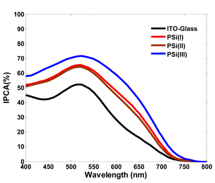
IPCE versus wavelength for DSSCs employing different PSi samples.
It is noteworthy that the introduction of PSi photoanode into the DSSC not only improves the LHE but also reduces the electron–hole recombination rate in the TiO2 layer. Schematic diagrams for the possible electron transferring in two types of photoanode structures are shown in Fig. 9. In conventional photoanode (Fig. 9a), without macro-pore structures, electrons that are injected into TiO2 nanoparticles may transfer around and need a much longer transfer distance. But as depicted in Fig. 9b, PSi photoanodes due to their vertically aligned macro-pores provide more pathways for electrons without increasing their transport distance in the TiO2 layer, thus reducing the chance of charge recombination, which also means that the electrons transfer efficiently. For analyzing the charge transfer and recombination processes at the TiO2/dye/electrolyte/Pt interfaces in DSSCs, EIS measurements were performed under AM 1.5 solar illumination and the results are shown in Fig. 10. Two semicircles extending from total series resistance are observed in high and middle frequency regions (left to right). The small semicircle (ZCT) in the high frequency region is attributed to the impedance corresponding to the charge transfer process occurring at the electrolyte/Pt interface, while the large semicircle (ZTiO2) in the low frequency region is attributed to the charge transfer and recombination at the TiO2/dye/electrolyte interface [36-38]. As shown in Fig. 10, the radius of the large semicircle located in low frequency region in the Nyquist plots decreases for DSSCs employing PSi-based photoanode compared with ITO glass-based DSSC. The radius values are in the order of PSi(III) < PSi(II) < PSi(I) < ITO-glass, which indicates a decrease of the electron transfer impedance (ZTiO2) and an increase of charge transfer rate at this interface. This is how the vertically aligned macro-pores facilitate interfacial charge transfer and thus lower the charge recombination. In particular, the PSi(III)-based DSSC has the smallest interfacial impedance, which implies the fastest interfacial electron transfer and thereby rendering the highest power conversion efficiency.

Electron transfer through TiO2 nanoparticles in: (a) conventional photoanode, (b) PSi photoanode.
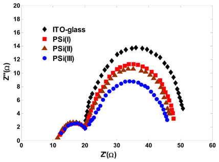
EIS spectra of DSSCs with various PSi photoanodes.
The fill factor (FF) is the ratio of the maximum power from the DSSC to the product of Voc and Jsc. The value of the FF depends on the normalized open circuit voltage [39]. A higher voltage will have a higher possible FF and the JV curve of the DSSC will be more approached a rectangle. The Voc is the difference between the Nernstian potential of the solution and the semiconductor’s quasi-Fermi level. At open circuit, the rates of electron injection and recombination/interception are equal, and their values determine the steady-state electron concentration in the semiconductor and therefore its quasi-Fermi level. The quasi-Fermi level, and thus Voc, can be increased by enhancing the rate of electron injection (Jsc) or decreasing the rate of electron recombination/interception. In the case of our devices, as shown in table 2, cells incorporated with PSi exhibit higher Voc and thus FF. This can be attributed to the following factors: first, as depicted in Fig. 6 and 7, PSi structures drastically suppress light reflection and enhance dyeloading capacity. These properties provide the photons with more opportunities to be absorbed by the dye molecules, results in a significant improvement in the rate of electron injection. Second, as shown in Fig. 10, the charge transfer impedance of the PSi based DSSCs is lower than that of the conventional DSSC. Thus, these results show that one can expect a lower recombination from the PSi electrode in comparison with the typical one.
4. Conclusion
This investigation presents a highly efficient and simple light trapping strategy by fabricating a novel macro-porous silicon based photoanode. The macroporous structures are prepared through a simple and cost effective electrochemical anodization method. The photoelectric measurements showed that the standard photovoltaic parameters for modified DSSCs including the short circuit current density, the fill factor, and the power conversion efficiency have remarkably increased compared with the values for a conventional DSSC. Among three different PSi geometries employed, the PSi(III) photoanode with more porosity percentage, shows the highest efficiency of 5.77 % which is nearly two times higher than that of the conventional one. Surface reflectance, dye adsorption, and electrochemical impedance spectroscopy experiments notified that the vertically aligned macro-pore structures are the origin of the light harvesting efficiency improvement. The total light reflection is dramatically reduced by the increase of the light path length inside these structures, which leads to more photon absorption. Moreover, porous structures with large surface area allow higher rate of dye adsorption and assist in the interfacial charge transfer, which render higher photocurrent and lower charge recombination. Further adjustments can be performed in future to achieve optimal light trapping structures, which provide a good way to improve the overall power conversion efficiency of DSSCs.
References
F. Sauvage, D. Chen, P. Comte, F. Huang, L. P Heiniger., Y. B. Cheng, R. A. Caruso and M. Gratzel, ACS Nano, 2010, 4(8), 4420-4425.
Sauvage F., Chen D., Comte P., Huang F., Heiniger. L. P, Cheng Y. B., Caruso R. A., Gratzel M.. ACS Nano 2010;4(8):4420–4425. 10.1021/nn1010396.T. K. Yun, S. S. Park, D. Kim, Y. K. Hwang, S. Huh, J. Y. Bae and Y. S. Won, J. Power Sources, 2011, 196(7), 3678-3682.
Yun T. K., Park S. S., Kim D., Hwang Y. K., Huh S., Bae J. Y., Won Y. S.. J. Power Sources 2011;196(7):3678–3682. 10.1016/j.jpowsour.2010.11.162.X.-D. Gao, X.-M. Li, X.-Y. Gan, Y.-Q. Wu, R.-K. Zheng, C.-L. Wang, Z.-Y. Gu and P. He, J. Mater. Chem., 2012, 22(36), 18930-18938.
Gao X.-D., Li X.-M., Gan X.-Y., Wu Y.-Q., Zheng R.-K., Wang C.-L., Gu Z.-Y., He P.. J. Mater. Chem. 2012;22(36):18930–18938. 10.1039/c2jm33945e.S. H. Ko, D. Lee, H. W. Kang, K. H. Nam, J. Y. Yeo, S. J. Hong, C. P. Grigoropoulos and H. J. Sung, Nano Lett., 2011, 11(2), 666-671.
Ko S. H., Lee D., Kang H. W., Nam K. H., Yeo J. Y., Hong S. J., Grigoropoulos C. P., Sung H. J.. Sung, Nano Lett. 2011;11(2):666–671. 10.1021/nl1037962.J. Qiu, F. Zhuge, X. Li, X. Gao, X. Gan, L. Li, B. Weng, Z. Shi and Y. H. Hwang, J. Mater. Chem., 2012, 22(8), 3549-3554.
Qiu J., Zhuge F., Li X., Gao X., Gan X., Li L., Weng B., Shi Z., Hwang Y. H.. J. Mater. Chem. 2012;22(8):3549–3554. 10.1039/c2jm15354h.S. M. Mahpeykar, J. Koohsorkhi and H. Ghafoori-fard, Nanotechnology, 2012, 23, 165602.
Mahpeykar S. M., Koohsorkhi J., Ghafoori-fard H.. Nanotechnology 2012;23:165602. 10.1088/0957-4484/23/16/165602.H. J. Koo, J. Park, B. Yoo, K. Yoo, K. Kim and N. G. Park, Inorg. Chim. Acta, 2008, 361, 677-683.
Koo H. J., Park J., Yoo B., Yoo K., Kim K., Park N. G.. Inorg. Chim. Acta 2008;361:677–683. 10.1016/j.ica.2007.05.017.K. Fan, W. Zhang, T. Peng, J. Chen and F. Yang, J. Phys. Chem. C, 2011, 115(34), 17213-17219.
Fan K., Zhang W., Peng T., Chen J., Yang F.. J. Phys. Chem. C 2011;115(34):17213–17219. 10.1021/jp204725f.X. Liu, M. Guo, J. Cao, J. Lin, Y. H. Tsang, X. Chen and H. Haung, Nanoscale Research Letters, 2014, 9, 362.
Liu X., Guo M., Cao J., Lin J., Tsang Y. H., Chen X., Haung H.. Nanoscale Research Letters 2014;9:362. 10.1186/1556-276X-9-362.N. C. Jeong, C. Prasittichai and J. T. Hupp, Langmuir, 2011, 27(23), 14609-14614.
Jeong N. C., Prasittichai C., Hupp J. T.. Langmuir 2011;27(23):14609–14614. 10.1021/la203557f.M. D. Brown, T. Suteewong, R. S. S. Kumar, V. D. Innocenzo, A. Petrozza, M. M. Lee, U. Wiesner and H. J. Snaith, Nano Lett., 2011, 11(2), 438-445.
Brown M. D., Suteewong T., Kumar R. S. S., Innocenzo V. D., Petrozza A., Lee M. M., Wiesner U., Snaith H. J.. Nano Lett. 2011;11(2):438–445. 10.1021/nl1031106.H. Choi, W. T. Chen and P. V. Kamat, ACS Nano, 2012, 6(5), 4418-4427.
Choi H., Chen W. T., Kamat P. V.. ACS Nano 2012;6(5):4418–4427. 10.1021/nn301137r.B. Mandlmeier, J. M. Szeifert, D. Fattakhova-Rohlfing, H. Amenitsch and T. Bein, J. Am. Chem. Soc., 2011, 133, 17274-17282.
Mandlmeier B., Szeifert J. M., Fattakhova-Rohlfing D., Amenitsch H., Bein T.. J. Am. Chem. Soc. 2011;133:17274–17282. 10.1021/ja204667e.A. Mihi, C. Zhang and P. V. Braun, Angew. Chem. Int. Ed., 2011, 50, 5712-5715.
Mihi A., Zhang C., Braun P. V.. Angew. Chem. Int. Ed. 2011;50:5712–5715. 10.1002/anie.201100446.W. Zhang, M. Anaya, G. Lozano, M. E. Calvo, M. B. Johnston, H. Miguez and H. J. Snaith, Nano Lett., 2015, 15, 1698-1702.
Zhang W., Anaya M., Lozano G., Calvo M. E., Johnston M. B., Miguez H., Snaith H. J.. Nano Lett. 2015;15:1698–1702. 10.1021/nl504349z.E. Yablonovitch and G. D. Cody, IEEE Trans. Electron Dev., 1982, 29(2), 300-305.
Yablonovitch E., Cody G. D.. IEEE Trans. Electron Dev. 1982;29(2):300–305. 10.1109/T-ED.1982.20700.P. Campbell and M. A. Green, J. Appl. Phys., 1987, 62(1), 243-249.
Campbell P., Green M. A.. J. Appl. Phys. 1987;62(1):243–249. 10.1063/1.339189.A. W. Smith and A. Rohatgi, Sol. Energy Mat. Sol. C., 1993, 29, 37-49.
Smith A. W., Rohatgi A.. Sol. Energy Mat. Sol. C 1993;29:37–49. 10.1016/0927-0248(93)90090-P.S. Q. Hussain, S. Ahn, H. Park, G. Kwon, J. Raja and Y. Lee, Vacuum, 2013, 94, 87-91.
Hussain S. Q., Ahn S., Park H., Kwon G., Raja J., Lee Y.. Vacuum 2013;94:87–91. 10.1016/j.vacuum.2013.01.026.L. Chen, M. M. Alkaisi and M. Y. Liao, J. Nonlinear Optic. Phys. Mat., 2010, 19, 761-766.
Chen L., Alkaisi M. M., Liao M. Y.. J. Nonlinear Optic. Phys. Mat. 2010;19:761–766. 10.1142/S0218863510005650.S. M. Kong, Y. Xiao, K. H. Kim, W. I. Lee and C. W. Chung, Thin Solid Films, 2011, 519, 3173-3176.
Kong S. M., Xiao Y., Kim K. H., Lee W. I., Chung C. W.. Thin Solid Films 2011;519:3173–3176. 10.1016/j.tsf.2011.01.251.S. Wooh, H. Yoon, J. Jung, Y. Lee, J. H. Koh, B. Lee, Y. S. Kang and K. Char, Adv. Mater., 2013, 25, 3111-3116.
Wooh S., Yoon H., Jung J., Lee Y., Koh J. H., Lee B., Kang Y. S., Char K.. Adv. Mater. 2013;25:3111–3116. 10.1002/adma.201300085.N. C. D. Nath, I. S. Jung, S.-W. Kim and J.-J. Lee, Sol. Energy, 2016, 134, 399-405.
Nath N. C. D., Jung I. S., Kim S.-W., Lee J.-J.. Sol. Energy 2016;134:399–405. 10.1016/j.solener.2016.05.008.C. H. Lee, P. T. Hsiao, M. D. Lu and J. M. Wu, RSC Adv., 2013, 3, 2216-2218.
Lee C. H., Hsiao P. T., Lu M. D., Wu J. M.. RSC Adv. 2013;3:2216–2218. 10.1039/c2ra22463a.C. Gerhards, C. Marckmann, R. Tolle, M. Spiegel, P. Fath, G. Willeke, E. Bucher, J. Creager and S. Narayanan, Proceedings of the 26th IEEE Photovoltaic Specialists Conference, 1997, 43-46.
Gerhards C., Marckmann C., Tolle R., Spiegel M., Fath P., Willeke G., Bucher E., Creager J., Narayanan S.. In : Proceedings of the 26th IEEE Photovoltaic Specialists Conference; 1997. p. 43–46.W. A. Nositschka, C. Beneking, O. Voigt and H. Kurz, Sol. Energy Mat. Sol. C., 2003, 76(2), 155-166.
Nositschka W. A., Beneking C., Voigt O., Kurz H.. Sol. Energy Mat. Sol. C. 2003;76(2):155–166. 10.1016/S0927-0248(02)00214-3.L. A. Dobrzanski, A. Drygała, K. Gołombek, P. Panek, E. Bielanska and P. Zieba, J. Mater. Process. Tech., 2008, 201(1-3), 291-296.
Dobrzanski L. A., Drygała A., Gołombek K., Panek P., Bielanska E., Zieba P.. J. Mater. Process. Tech. 2008;201(1-3):291–296. 10.1016/j.jmatprotec.2007.11.278.M. J. Sailor, Porous Silicon in Practice: Preparation, Characterization and Applications, Wiley, New York (2012).
Sailor M. J.. Porous Silicon in Practice: Preparation, Characterization and Applications Wiley. New York: (2012).A. Langner, F. Muller, U. Gosele, O. Hayden, K. Nielsch (Eds.), Molecular- and Nano-Tubes, Springer, New York, 431 (2011).
In : Langner A., Muller F., Gosele U., Hayden O., Nielsch K., eds. Molecular- and Nano-Tubes Springer. New York: (2011). p. 431.M. Nazari and S. Khatami, Sensor Mater., 2013, 25, 131-140.
Nazari M., Khatami S.. Sensor Mater. 2013;25:131–140.S. Ito, T. N. Murakami, P. Comte, P. Liska, C. Gratzel, M. K. Nazeeruddin and M. Gratzel, Thin Solid Films, 2008, 516, 4613-4619.
Ito S., Murakami T. N., Comte P., Liska P., Gratzel C., Nazeeruddin M. K., Gratzel M.. Thin Solid Films 2008;516:4613–4619. 10.1016/j.tsf.2007.05.090.Y. S. Jin, K. H. Kim and H. W. Choi, J. Korean Phys. Soc., 2010, 57, 1049-1053.
Jin Y. S., Kim K. H., Choi H. W.. J. Korean Phys. Soc. 2010;57:1049–1053. 10.3938/jkps.57.1049.A. Sharma, R. K. Karn and S. K. Pandiyan, Int. J. Appl. Eng. Res., 2013, 8, 2057-2066.
Sharma A., Karn R. K., Pandiyan S. K.. Int. J. Appl. Eng. Res. 2013;8:2057–2066.M. Aliaghayee, H. Ghafoori Fard and A. Zandi, J. Porous Mater., 2015, 22, 1617-1626.
Aliaghayee M., Ghafoori Fard H., Zandi A.. J. Porous Mater. 2015;22:1617–1626. 10.1007/s10934-015-0045-3.N.-G. Park, J. van de Lagemaat and A. J. Frank, J. Phys. Chem. B, 2000, 104, 8989-8994.
Park N.-G., van de Lagemaat J., Frank A. J.. J. Phys. Chem. B 2000;104:8989–8994.J. Bisquert, Phys. Chem. Chem. Phys., 2000, 2, 4185-4192.
Bisquert J.. Phys. Chem. Chem. Phys. 2000;2:4185–4192. 10.1039/b001708f.R. Kern, R. Sastrwan, J. Ferber, R. Stangl and J. Luther, Electrochim. Acta., 2002, 47, 4213-4225.
Kern R., Sastrwan R., Ferber J., Stangl R., Luther J.. Electrochim. Acta. 2002;47:4213–4225. 10.1016/S0013-4686(02)00444-9.Q. Wang, J.-E. Moser, and M. Gratzel, J. Phys. Chem. B, 2005, 109, 14945-14953.
Wang Q., Moser J.-E., Gratzel M.. J. Phys. Chem. B 2005;109:14945–14953. 10.1021/jp052768h.M. A. Green, Solid State Electronics, 1981, 24, 788-789.
Green M. A.. Solid State Electronics 1981;24:788–789. 10.1016/0038-1101(81)90062-9.