Preparation of Tantalum Anodic Oxide Film in Citric Acid Solution - Evidence and Effects of Citrate Anion Incorporation
Article information
Abstract
Tantalum anodic oxide film was prepared in citric acid solution of various concentrations and the prepared Ta anodic oxide film was characterized by various electrochemical techniques and X-ray photoelectron spectroscopy (XPS). The prepared Ta anodic oxide film showed typical n-type semiconducting properties and the dielectric properties were strongly dependent on the citric acid concentration. The variation of electrochemical and electronic properties was explained in terms of electrolyte anion incorporation into the anodic oxide film, which was supported by XPS measurements.
1. Introduction
The conventional gate oxide materials based on SiO2 have reached their physical limitations in terms of scaling down for the needs of microelectronics, because of the SiO2 (ε = 3.9) film with the thickness less than 3 nm shows leakage currents due to the direct tunneling.1) A practical approach to overcome this problem is to use high dielectric materials such as metal oxide with thicker films with capacitance similar to SiO2 layers.
Tantalum pentoxide (Ta2O5) is one of the best candidates for a high performance dielectric material to be used in various electronic devices2-8) because of its superior electronic properties such as high dielectric constant (amorphous: 29.2~29.52) and crystalline: 45.6~51.72)), low dielectric loss and low leakage current as well as good chemical and thermal stabilities.
Various methods have been developed to produce Ta2O5 thin film. Atomic layer deposition (ALD) enables one to control the thin film thickness very precisely and grow films with uniform thickness and free of impurities even on profiled substrates.9-12) Photoinduced chemical vapor deposition has received much attention since it operates at low temperature, which minimizes problems such as atomic diffusion, dopant redistribution, and defect generation caused by higher temperature and also the processed surface is not subject to the damaging ionic bombardment, which is inevitable in plasma assisted methods.13,14) Ion beam sputtering deposition (IBSD) is an atom-by-atom (or molecule-by-molecule) transport process of high energy materials in a relatively cold and high vacuum environment, resulting in a film with a high packing density and low optical scattering.15,16)
Ta2O5 can be also grown electrochemically by anodic polarizedation in various aqueous solutions. Anodic oxide grows on bulk tantalum metal by the simultaneous movements of oxygen and tantalum ions through the oxide layer and this electrochemical procedure is very promising for economical preparation of Ta2O5.
Since both oxygen and Ta ions can be moved, the oxide growth may take place at two, i.e., Ta|oxide and oxide|electrolyte, interfaces and the prepared Ta oxide may consist of two layers of the different structures and properties. The inner layer should be composed of relatively pure oxide while the outer layer contains anion contaminants from the electrolyte. In an early study, Randall et al. proved the movements of tantalum ion to form outer oxide layer with electrolyte incorporation and oxygen to grow inner oxide layer by a radioactive tracer technique.17)
The properties of the outer oxide layer should be strongly affected by the electrolyte and its concentration because the electrolyte is incorporated into the outer oxide layer. It was reported that phosphoric acid is readily incorporated and the dielectric and ionic conduction properties of the outer layer of the anodic film is affected more strongly by incorporated phosphate anion than incorporated sulphate anion.18-20) We have shown that nanosized patterns of tantalum oxide can be grown by applying a bias between a tip of current sensing AFM and Ta surface in an ambient condition based on electrochemical mechanism.21)
In this paper, tantalum anodic oxide film was grown in citric acid solution and the characterization of the prepared Ta anodic oxide film by various electrochemical techniques and X-ray photoelectron spectroscopy (XPS) proved the incorporation of citrate anion during the anodic oxide growth. The prepared Ta anodic oxide film showed typical n-type semiconducting properties and the dielectric properties were found to be strongly affected by the citric acid concentration.
2. Experimental
Tantalum anodic oxide film was grown on tantalum foil. Prior to electrochemical anodization, tantalum foil was mechanically polished with diamond slurries of 1, 0.5, 0.25, and 0.125 mm sequentially, degreased with dichloromethane overnight and then rinsed with Milli-Q water (Millipore, 18 MW·cm). Electrochemical anodization was carried out in citric acid aqueous solutions of various concentrations (0.01, 0.05, 0.1, and 0.2 M). A conventional single compartment three-electrode electrochemical cell with a Ag/AgCl reference electrode and a platinum foil counter electrode was used. All the potentials are presented with respect to Ag/AgCl unless otherwise stated. The apparent electrode area was 0.283 cm2.
For anodic polarization, a potentiostat (Toho Technical Research Potentiostat/ Galvanostat 2001) connected with a function generator (Hokuto Denko Ltd.) was used and for AC impedance measurements, a frequency response analyzer (NF Electronics Instruments) with personal computer control was used. Experiments were performed as follows. Initially, tantalum foil was anodized up to 2 V (vs. Ag/AgCl) galvanostatically at current density of 0.1 mA/cm2 and then stabilized potentiostatically at the same potential for 30 minutes. Then, cyclic vol tammetry (sweep rate: 50 mV/s) and AC impedance measurement were carried out in the same solution. After the electrochemical measurements at 2 V were completed, anodization and the electrochemical characterizations were carried out at 4 V in the same manner as at 2 V. These steps were repeated every 2 V until the applied potential of 10 V was reached.
Finally, obtained Ta anodic films were examined by XPS (Rigaku XPS 7000) with Mg-Kα X-ray source (1253.6 eV). All the binding energy was calibrated with a C1s peak at 285.0 eV. Depth profiling was performed by Ar+ ion sputtering with current density of 1000 mA/cm2 and acceleration voltage of 500 V. With these Ar+ ion sputtering parameters, etching rate was estimated to be 0.41 nm/s. The thickness of the oxide layer was determined by spectroscopic ellipsometry (GESP-5, SOPRA) using a 30 W Xe lamp as a light source.
3. Results and Discussion
Figure 1 shows a typical cyclic voltammogram of the tantalum anodic oxide film prepared at 10 V in a 0.1 M citric acid solution. While cathodic current due to hydrogen evolution flew in negative potential region and became significant at ca. −0.5 V, no evident current was observed in the positive potential region, showing that the tantalum anodic oxide film is an n-type semiconductor.22) The anodic current peak observed around −0.75 V should be due to the oxidation of hydrogen.

A typical cyclic voltammogram of a tantalum anodic oxide, which was prepared in a 0.1 M citric acid aqueous solution at 10 V, measured in the same solution. Sweep rate: 50 mV/s.
Figure 2 shows Cole-Cole plots of the Ta anodic oxide, which was prepared at the preparation potential of 10 V in 0.1 M citric acid aqueous solution, measured −0.85, −0.60, 0.0, and +1.50 V. AC impedance measurements also showed n-type semiconducting property, supporting the result of the cyclic voltammetry. While the perpendicular lines were observed at the positive potential region due to the high resistance of the oxide film, well-defined semicircles at −0.60 and –0.85 V were appeared, respectively, and these semicircles were attributed to the hydrogen evolution reaction. It was reported that the thin layers (less than 15 nm) of tantalum anodic oxide are supposed to behave as an n-type semiconductor with oxygen vacancies acting as donor sites but the thicker films act as an insulator.23)
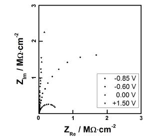
Cole-Cole plots of a tantalum anodic oxide film, which was prepared on a Ta substrate at 10 V in 0.1 M citric acid aqueous solution, measured at the applied potential of –0.85, -0.60, 0.0, and +1.50 V (vs. Ag/AgCl).
Figure 3(a)-(c) shows XP spectra of a prepared Ta anodic oxide grown on a tantalum foil in a 0.1 M citric acid aqueous solution at the preparation potential of 10 V in C1s, O1s, and Ta4f regions, respectively, after Ar+ ion sputtering of 0~50 s. Fig. 3(a) shows that even after 20 s Ar+ ion sputtering, the C1s peak is still apparent, although its intensity is very weak. While the C1s peak before Ar+ ion sputtering is attributable to the surface organic contaminants, the weak C1s peak with smaller binding energy after the sputtering should be due to citrate anion incorporated into the anodic oxide film during electrochemical anodization. Peak intensity of O1s signal decreased gradually as sputtering time increased as shown in Fig. 3(b). There are two possibilities for this decrease. One is the decrease of oxygen content, i.e., increase of oxygen deficiency, in deeper region of tantalum anodic oxide film and the other is the reduction of tantalum oxide by Ar+ ion sputtering. The reduction of tantalum oxide is clearly seen in the depth dependent XP spectra in Ta4f region as shown in Fig. 3(c). While only strong Ta5+ doublet peaks were observed at the as-grown tantalum oxide without sputtering, showing the oxide was essentially Ta2O5, the intensities of the doublet peaks due to Ta5+ became very weak even just after 10 s sputtering and further decreased with sputtering time. On the other hand, those due to metallic Ta (Ta0) grew with sputtering time.
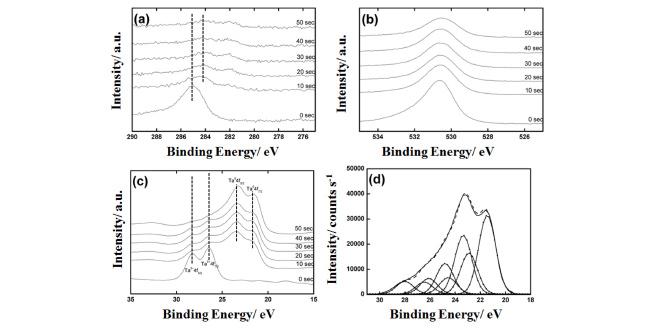
XP spectra of a tantalum anodic oxide film, which was prepared in a 0.1 M citric acid aqueous solution at 10 V, in (a) C1s, (b) O1s, and (c) Ta4f regions after various Ar+ ion sputtering time, and in (d) Ta4f region after 50s Ar+ ion sputtering with deconvolution.
Figure 3(d) shows XP spectrum of the Ta anodic film in Ta4f region after 50s Ar+ ion sputtering with deconvolution. For the deconvolution, the spin-orbit doublet separation of 1.9 eV, the full width at halfmaximum (FWHM) value of 1.35 eV, and the intensity ratio (Ta4f7/2/Ta4f5/2) of 4/3 were used in all peak assignments.23) The Ta4f deconvoluted XPS spectrum was divided into four kinds of tantalum doublet peaks. The peaks at the binding energies of 21.5 eV and 26.1 eV were assigned as Ta0 7/2 and Ta5+ 7/2, respectively. The peaks at the binding energies of 22.9 eV and 24.9 eV indicate the existence of sub-oxide states and were denoted as ox1 and ox2, respectively, which may be TaO and TaO2, respectively,23) although the origin of these sub-oxide states is rather ambiguous because these sub-oxide peaks possibly came from the native oxide layer and/or from the reduction process of Ta2O5 by Ar+ ion sputtering. It is generally believed that the sub-oxide acts as donor sites in the tantalum anodic oxide, which should be the origin of n-type semiconducting property of the Ta anodic oxide thin film,23) and the different oxidation states can be caused by the oxidation conditions.24)
XPS results suggest the incorporation of citrate anion into the anodic oxide layer. It is practically well known that anion is readily incorporated into Ta anodic oxide and it is suggested that incorporated anions behave as defect sites in the oxide phase, resulting in alteration of dielectric properties of anodic film from the pure Ta oxide layer.17-19) Recently, Di Franco et al. reported the nitrogen incorporation into anodic Ta2O5 layer from a bath containing ammonium ions.25) Thus, it is expected that the electronic properties of the anodic Ta2O5 film must be affected by anion incorporation, which might be dependent on the electrolyte concentrations. To clarify the effect of citrate anions included in the Ta anodic oxide film, AC impedance measurements were carried out at the Ta anodic oxide films prepared in 0.01, 0.05, 0.1, and 0.2 M citric acid solutions.
One of the most important features of AC impedance study was the frequency dispersion. Different to the crystalline semiconductors, in case of amorphous metal oxide films, frequency dispersion is normally expected owing to the influence of the ionized states to space charge capacitance. For that reason, the AC impedance measurement is dependent not only to the potential distribution but also to the density of states (DOS) distribution of local states in the anodic film because of the deep levels act as charge storage in the forbidden band. Lu et al. explained this frequency dependence of Ta anodic oxide as constant phase element (CPE) caused by the inhomogeneous composition owing to the phosphate ion incorporation.26) Surface roughness, inhomogeneous composition, and reaction rate variation depending on the plane orientation are the major contribution to CPE.27-29)Fig. 4 shows imaginary part of admittance as a function of angular frequency, ω (= 2πf), in the frequency range of 1 Hz ~ 1 kHz.
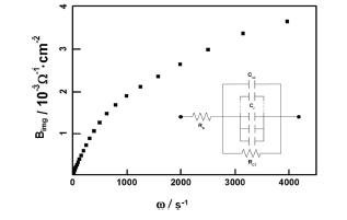
Imaginary part of admittance of a tantalum anodic oxide film, which was prepared on a Ta substrate at 10 V in 0.1M citric acid solution, as a function of angular frequency. Inset: Equivalent circuit used for analyses. See text for details.
To explain frequency dispersion behavior of Ta anodic oxide, we considered the existence of electronic states due to defect sites below the conduction band in space charge layer of amorphous anodic oxide on tantalum.30) Since a finite response time is needed for the electron capture and emission reaction between the conduction band and the localized states, the local states cannot contribute to the capacitance as a charge storage if the frequency of the imposed AC signal is faster than the relaxation time. Because each discrete local state has different relaxation time, which depends on the energy difference between the conduction band and the given local state, and, therefore, the total capacitance is a function of the applied AC frequency. Based on the above model with an equivalent circuit shown as inset of Fig. 4, the imaginary part of the admittance, B, can be given by:
where ω is the angular frequency, CSC is the space charge capacitance, and Ci and τ are the capacitance and time constant of other charge accumulation components parallel to the space charge layer, i.e., local states.31) The second term in the right hand side of Eq. (1) becomes constant at high frequency region and the space charge capacitance can be obtained from the slope of the linear portion of the B-ω plot (Fig. 4). In many semiconductor electrodes, the double layer capacitance can be neglected because it is normally in the range of 10-40 μF/cm2 and is much larger than the space charge capacitance.
Figure 5 shows the relations between the differential capacitance and the applied potential of Ta anodic oxide films grown on tantalum foils at various preparation potentials (2, 4, 6, 8, 10 V, vs. Ag/AgCl) in citric acid solutions of (a) 0.01, (b) 0.05, (c) 0.1, and (d) 0.2 M obtained from impedance analyses. In all the cases, the interfacial capacitance increased as potential became more negative than ca. 0 V and is almost constant in more positive potential region. This behavior can be explained by using the following equation, which applicable to a parallel-plate capacitor.
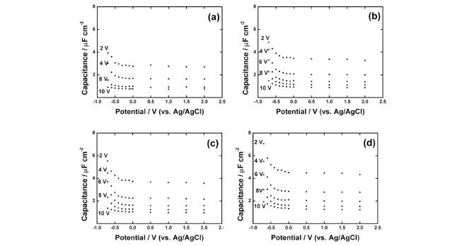
Potential dependencies of differential capacitance of tantalum anodic oxide films, which were prepared at various potentials in (a) 0.01 M, (b) 0.02 M, (c) 0.1 M, and (d) 0.2 M citric acid solutions.
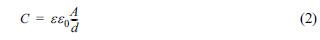
where ε is the dielectric constant of the material between the plates, ε0 is the permittivity of the free space, A is the area, and d is the thickness between the plates. As the thickness of a capacitor is decreased, the capacitance is increased. Likewise, by treating the space charge layer of a semiconductor as a parallel plate capacitor, the space charge capacitance of a semiconductor should be closely related to the thickness of the space charge layer.
The energy diagrams of Ta/Ta2O5/electrolyte interface at (a) the flat band potential, (b) small reverse bias where the space charge layer thickness is less than the oxide thickness, and (c) large reverse bias where the space charge layer thickness becomes equal to the oxide thickness are schematically shown in Fig. 6 together with typical Mott-Schottky plot, i.e., the relation between CSC −2 and potential. When the applied potential is made positive from the flat band potential, the thickness of the space charge layer increases and, therefore, the capacitance decreases (Fig. 6(b), c.f. Eq. (2)). When potential is made more positive, the thickness of the space charge layer increases further and finally becomes equal to the thickness of the anodic oxide film (Fig. 6(c)) and the capacitance is reached to its minimum value. Since the thickness of the space charge layer cannot exceed the thickness of the oxide film and, therefore, does not increase further even if more positive potential is applied, the capacitance remains constant in more positive potential region (Fig. 6(c)).
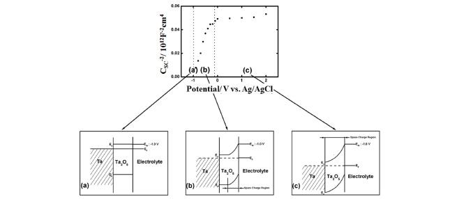
Schematic energy diagrams of Ta/Ta2O5/electrolyte interface at (a) the flat band potential, (b) small reverse bias where the space charge layer thickness is less than the oxide thickness, and (c) large reverse bias where the space charge layer thickness becomes equal to the oxide thickness together with a typical Mott-Schottky plot, i.e., the relation between CSC -2 and potential.
The higher the citric acid concentration, the higher the interfacial capacitances including the constant capacitance in positive potential region at the tantalum anodic oxide films regardless of the preparation potentials as shown in Fig. 7 where the interfacial capacitances of the tantalum anodic oxide films prepared at various potentials were plotted against citric acid concentration. This result suggests that the effective dielectric constant is affected by the electrolyte concentration. Li et al. reported that the dielectric constant of oxide is affected by the amount of anion incorporated into the anodic oxide film.32) It is reasonable to consider that the amount of anion incorporated into the anodic oxide film is higher as the electrolyte concentration is increased. As a result, the ionic species in the oxide film would increase the DOS of the local states, which in turn influence the differential capacitance. The possible reason why the interfacial capacitance against citric acid concentration plot is deviated from the linearity at higher concentration is that the amount of incorporated citrate anion is not linearly dependent on the citric acid concentration.

Interfacial capacitances of tantalum anodic oxide films, which were prepared in citric acid solutions of various concentrations at various potentials, as a function of citric acid concentration.
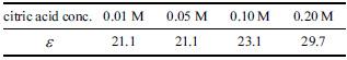
The concentration dependent dielectric constant can be calculated using Eq. (2). The thickness of the Ta anodic oxide is known to be linearly related to the preparation potential33) and that of the Ta anodic oxide prepared at 10 V in citric acid solution is determined to be ca. 22 nm by ellipsometry regardless of citric acid concentration. Thus, the thickness of the Ta anodic oxide prepared at any potential in this study was estimated by using the value of 2.2 nm/V. The dielectric constants of the oxide films prepared in citric acid solutions of various concentrations were calculated using the estimated thicknesses and the values of ε0 = 8.85 × 10⁻¹² F/m and A = 0.283 cm2 and are shown in Table 1. It is clear that the dielectric constant of the anodic oxide film increases as the concentration of citric acid solution increases, supporting the above discussions.
Dielectric constants of tantalum anodic oxide films prepared in various citric acid electrolyte concentrations (Eprep =10V).
4. Conclusions
Tantalum anodic oxide film was grown in citric acid solutions of various concentrations. Cyclic voltammogram of the Ta anodic oxide film showed cathodic current due to hydrogen evolution, which became significant at potentials more negative than ca. −0.5 V but no evident anodic current in positive potential region, which are the typical characteristics of n-type semiconductor electrode. Impedance analyses confirmed that the prepared Ta anodic oxide film behaved as n-type semiconductor.
The tantalum anodic oxide film showed strong frequency dispersion in the measured frequency range. It was attributed to the existence of electronic states due to defect sites below the conduction band in the space charge layer. Differential capacitance showed very strong dependence to the citric acid electrolyte concentration as more citrate anions were incorporated into tantalum anodic oxide film prepared in more concentrated electrolyte solution, suggesting that the incorporated citrate anions induce the local states in the forbidden band, which act as charge reservoir. Incorporation of citrate anion during the anodic oxide growth was proved by XPS.
References
S. Boughaba, M. Islam, J. P. McCaffrey, G. I. Sproule, and M.J. Graham, Thin Solid Films 371, 119 (2000).
Boughaba S., Islam M., McCaffrey J. P., Sproule G. I., Graham M.J.. Thin Solid Films 2000;371:119. 10.1016/S0040-6090(00)00982-2.P. C. Joshi and M. W. Cole, J. Appl. Phys. 86, 871 (1999).
Joshi P. C., Cole M. W.. J. Appl. Phys. 1999;86:871. 10.1063/1.370817.Y. Nakagawa and T. Okada, J. Appl. Phys. 68, 556 (1990).
Nakagawa Y., Okada T.. J. Appl. Phys. 1990;68:556. 10.1063/1.346828.S. Tanimoto, M. Matsui, K. Kamisako, K. Kuroiwa, and Y. Tarui, J. Electrochem. Soc. 139, 320 (1992).
Tanimoto S., Matsui M., Kamisako K., Kuroiwa K., Tarui Y.. J. Electrochem. Soc. 1992;139:320. 10.1149/1.2069193.Y. Nishimura, K. Tokunaga, and M. Tsuji, Thin Solid Films 226, 144 (1993).
Nishimura Y., Tokunaga K., Tsuji M.. Thin Solid Films 1993;226:144. 10.1016/0040-6090(93)90220-J.K. W. Kwon, C. S. Kang, S. O. Park, H. K. Kang, and S. T. Ann, IEEE Trans. Electron Devices 43, 919 (1996).
Kwon K. W., Kang C. S., Park S. O., Kang H. K., Ann S. T.. IEEE Trans. Electron Devices 1996;43:919. 10.1109/16.502124.J. Y. Zhang, B. Lim, V. Dusastre, and I. W. Boyd, Appl. Phys. Lett. 73, 2299 (1998).
Zhang J. Y., Lim B., Dusastre V., Boyd I. W.. Appl. Phys. Lett. 1998;73:2299. 10.1063/1.121803.Y. Yang, P. Sheridan, and W. Lu, Appl. Phys. Lett. 100, 203112 (2012).
Yang Y., Sheridan P., Lu W.. Appl. Phys. Lett. 2012;100:203112. 10.1063/1.4719198.M. Vehkamäki, T. Hatanpää, T. Hänninen, M. Ritala, and M. Leskelä, Electrochem. Solid-State Lett., 2, 504 (1999).
Vehkamäki M., Hatanpää T., Hänninen T., Ritala M., Leskelä M.. Electrochem. Solid-State Lett. 1999;2:504. 10.1149/1.1390884.T. Suntola, Thin Solid Films 216, 84 (1992).
Suntola T.. Thin Solid Films 1992;216:84. 10.1016/0040-6090(92)90874-B.J. Aarik, A. Aidla, T. Uustare, and V. Sammelselg, J. Crystal Growth 148, 268 (1995).
Aarik J., Aidla A., Uustare T., Sammelselg V.. J. Crystal Growth 1995;148:268. 10.1016/0022-0248(94)00874-4.D. M. Hausmann, P. de Rouffignac, A. Smith, R. Gordon, and D. Monsma, Thin Solid Films 443, 1 (2003).
Hausmann D. M., de Rouffignac P., Smith A., Gordon R., Monsma D.. Thin Solid Films 2003;443:1. 10.1016/S0040-6090(03)00502-9.J. Y. Zhang, B. Hopp, Z. Geretovszky, and I. W. Boyd, Appl. Surf. Sci. 168, 307 (2000).
Zhang J. Y., Hopp B., Geretovszky Z., Boyd I. W.. Appl. Surf. Sci. 2000;168:307. 10.1016/S0169-4332(00)00768-6.M. Tsuchiya, S.K.R.S. Sankaranarayanan, and S. Ramanathan, Prog. Mater. Sci. 54, 981 (2009).
Tsuchiya M., Sankaranarayanan S.K.R.S., Ramanathan S.. Prog. Mater. Sci. 2009;54:981. 10.1016/j.pmatsci.2009.04.003.C. C. Lee, J. C. Hsu, and D. H. Wong, Appl. Surf. Sci. 171, 151 (2001).
Lee C. C., Hsu J. C., Wong D. H.. Appl. Surf. Sci. 2001;171:151. 10.1016/S0169-4332(00)00556-0.W. Kulisch, D. Gilliland, G. Ceccone, H. Rauscher, L. Sirghi, P. Colpo, and F. Rossi, J. Vac. Sci. Technol. A 26, 991 (2008).
Kulisch W., Gilliland D., Ceccone G., Rauscher H., Sirghi L., Colpo P., Rossi F.. J. Vac. Sci. Technol. A 2008;26:991. 10.1116/1.2832407.J. J. Randle, W. J. Bernard, and R. R. Wilkinson, Electrochim. Acta 10, 183 (1965).
Randle J. J., Bernard W. J., Wilkinson R. R.. Electrochim. Acta 1965;10:183. 10.1016/0013-4686(65)87018-9.C. J. Dell’Oca and L. Young, J. Electrochem. Soc. 117, 1548 (1970).
Dell’Oca C. J., Young L.. J. Electrochem. Soc. 1970;117:1548. 10.1149/1.2407380.Y. M. Li and L. Young, Electrochim. Acta 44, 605 (1998).
Li Y. M., Young L.. Electrochim. Acta 1998;44:605. 10.1016/S0013-4686(98)00183-2.J. D. Sloppy, N. J. Podraza, E. C. Dickey, and D. D. Macdonald, Electrochim. Acta 55, 8751 (2010).
Sloppy J. D., Podraza N. J., Dickey E. C., Macdonald D. D.. Electrochim. Acta 2010;55:8751. 10.1016/j.electacta.2010.07.077.Y. Kim, J. Zhao, and K. Uosaki, J. Appl. Phys. 94, 7733 (2003).
Kim Y., Zhao J., Uosaki K.. J. Appl. Phys. 2003;94:7733. 10.1063/1.1627951.V. Macagno and J. W. Schultze, J. Electroanal. Chem. 180, 157 (1984).
Macagno V., Schultze J. W.. J. Electroanal. Chem. 1984;180:157. 10.1016/0368-1874(84)83577-7.O. Kerrec, D. Devilliers, H. Groult, and P. Marcus, Mat. Sci. and Eng. B 55, 134 (1998).
Kerrec O., Devilliers D., Groult H., Marcus P.. Mat. Sci. and Eng. B 1998;55:134. 10.1016/S0921-5107(98)00177-9.S. Lecuyer, A. Quemerais, and G. Jezequel, Surf. Interface Anal. 18, 257 (1992).
Lecuyer S., Quemerais A., Jezequel G.. Surf. Interface Anal. 1992;18:257. 10.1002/sia.740180403.F. Di Franco, M. Santamaria, F. Di Quarto, E. Tsuji, and H. Habazaki, Electrochim. Acta 59, 382 (2012).
Di Franco F., Santamaria M., Di Quarto F., Tsuji E., Habazaki H.. Electrochim. Acta 2012;59:382. 10.1016/j.electacta.2011.10.086.Q. Lu, S. Mato, P. Skeldon, G. E. Thompson, and D. Masheder, Thin Solid Films 429, 238 (2003).
Lu Q., Mato S., Skeldon P., Thompson G. E., Masheder D.. Thin Solid Films 2003;429:238. 10.1016/S0040-6090(02)01292-0.O. Kerrec, D. Devilliers, H. Groult, and M. Chemla, Electrochimica Acta. 40, 719 (1995).
Kerrec O., Devilliers D., Groult H., Chemla M.. Electrochimica Acta 1995;40:719. 10.1016/0013-4686(94)00330-4.G. E. Cavigliasso, M. J. Esplandiu, and V. A. Macagno, J. Appl. Electrochem. 28, 1213 (1998).
Cavigliasso G. E., Esplandiu M. J., Macagno V. A.. J. Appl. Electrochem. 1998;28:1213. 10.1023/A:1003449917148.Impedance Spectroscopy, J. R. Macdonald ed., p. 90, John Wiley & Sons, New York (1987).
Macdonald J. R.. Impedance Spectroscopy 1987. New York: John Wiley & Sons.F. Di Quarto, S. Piazza, and C. Sunseri, Electrochimca. Acta 35, 99 (1990).
Di Quarto F., Piazza S., Sunseri C.. Electrochimca. Acta 1990;35:99. 10.1016/0013-4686(90)85045-O.M. Tomkiewicz, J. Electrochem. Soc. 126, 2220 (1979).
Tomkiewicz M.. J. Electrochem. Soc. 1979;126:2220. 10.1149/1.2128931.Y. M. Li and L. Young, J. Electrochem. Soc. 147, 1344 (2000).
Li Y. M., Young L.. J. Electrochem. Soc. 2000;147:1344. 10.1149/1.1393360.C. J. Dell’Oca, D. J. Pulfrey, and L. Young, in Physics of Thin Films, M. H. Francombe and R. W. Hoffmann ed., Vol. 6, Academic, New York and London (1971).
Dell’Oca C. J, Pulfrey D. J, Young L. in Physics of Thin Films, M. H. Francombe and R. W. Hoffmann ed. 1971. New York and London: Academic.