


1. Introduction
Two hundred years ago, less than one billion people lived on Earth. Nowadays, according to the United Nations (UN), humans have exceeded the 7 billion on the planet [1]. This increase in the world population, together with the economic growth of some countries, has triggered an abrupt increase in global energy consumption. Currently, 80% of the total energy available on the planet requires the combustion of fossil fuels for its production, which is not a clean and sustainable approach [2]. In addition, fossil fuels are non-renewable, which motivates the study and development of systems for energy generation based on renewable sources (e.g. sunlight or wind) and that are environmentally friendly.
In this context, an attractive alternative to fossil fuels is hydrogen [3-5], which is one of the most abundant chemical elements, constituting 75% of the mass and 90% of the atoms in the universe [6]. It is not considered a direct source of energy, but an energy vector (a form, in this case, chemical, that can be used to store or transport energy). Nowadays, ca. 96% of world hydrogen production is by steam reforming of natural gas.
In this regard, photoelectrochemical water splitting with a sunlight source and a suitable semiconductor photoelectrode has emerged as a promising and sustainable pollutant-free hydrogen production method [7-9]. The hydrogen produced at the cathode of the photoelectrochemical cell (PEC) is stored and subsequently used in a fuel cell stack or another similar device to satisfy the portable (e.g. electronic devices or transportation) or stationary (e.g. power station) electricity demand. The advantage of this alternative is that solar energy is used directly to produce hydrogen, which means having a simple system operation and probably decreased implementation costs [10]. Fig. 1 shows a diagram of water splitting in a PEC.
A primary matter in the fabrication of a PEC is the selection of an efficient (light to chemical energy conversion) and stable (underwater photoelectrolysis conditions) material for the photoelectrode(s). The anode and/or cathode of these cells are fabricated using semiconductor materials capable of absorbing the energy of the photons in the regions of ultraviolet and (some of them) visible wavelengths, promoting the half-reactions in Eq. (1) and/or (2) at the electrode(s) | electrolyte interface.
Anode half-reaction:
Cathode half-reaction:
Three materials have received particular attention for the fabrication of photoanodes for photoelectrochemical cells: (1) titanium dioxide (TiO2), (2) hematite (╬▒-Fe2O3), and (3) tungsten trioxide (WO3). These materials present high efficiencies for solar energy capture and conversion to chemical energy, stability under water splitting operating conditions, and/or low cost and earth abundance [11]. However, when operating under illumination in the visible range (ca. 45% of the solar spectrum), most of these semiconductors need an external potential (bias) to promote the oxygen evolution reaction on their surface, due to the position of their conduction and valence bands [12]. This limitation restricts the use of these materials in a practical way, so the search for new materials is still under study.
In the search for new semiconductor materials to fabricate photoanodes to drive the water splitting reaction (WSR), molybdenum oxides have emerged as a promising option. Some compounds of the MoOx family have been reported to have the following properties: (1) stability under acidic conditions, (2) n-type semiconduction, (3) relative band edge positions in aqueous electrolytes, and (4) ban-dgap energy values (Eg > 1.23 eV) suitable for harvesting enough energy to drive the oxygen evolution reaction (OER) in a PEC [13-15].
Many deposition techniques, such as evaporation [16], chemical vapor deposition [17], sputtering [18,19], and various wet chemistry methods, such as sol-gel spin coatings processes [20], electrodeposition [13], and spray pyrolysis [21], have been used to prepare MoOx films. Among these, the electrodeposition technique provides a simple, inexpensive, and scalable way to fabricate semiconductor materials.
On the other hand, considering that pure molybdenum cannot be electrodeposited from aqueous solutions, the co-deposition of this metal with other metals such as nickel and/or tungsten to produce metallic alloys has been widely studied [22,23]. In this regard, the use of nickel as a catalyst has become increasingly popular in recent years [24]. It is well known that the presence of nickel in electrodes provides catalytic activity for both the oxygen and hydrogen evolution reactions in an aqueous solution, which, combined with the properties listed above for molybdenum oxides, makes the idea of studying photoelectrodes based on mixed molybdenum-nickel oxides appealing.
In this work, undoped and nickel-doped molybdenum oxide photoanodes were fabricated by electrodeposition. The structure and morphology of these electrodes were studied by scanning electron microscopy (SEM) and atomic force microscopy (AFM). The compositional analysis was performed by Energy-dispersive X-ray spectroscopy (EDS or EDX) and X-ray photoelectron spectroscopy (XPS). Finally, the optical and photoelectrochemical characterization of these photoanodes was performed by UV-Visible spectroscopy and linear scanning voltammetry (LSV), respectively.
2. Experimental
2.1. Electrodeposition of molybdenum oxides films
A solution (hereinafter named solution S2) containing 0.075 M of molybdenum trioxide (MoO3, 99.97% purity, Sigma Aldrich), 0.075 M of nickel (NiSO4┬Ę6H2O, 99.00% purity, Merck), 0.50 M of sodium citrate (Na3C6H5O7┬Ę2H2O, 99.00% purity, Merck) and 0.70 M of ammonium hydroxide (NH4OH, 25% NH3 in H2O, Merck) was used as an electrolyte for the electrodeposition of thin (nanometric) films of molybdenum oxide (s) doped with nickel on FTO-coated glass.
Electrodeposition experiments done with a similar electrolyte solution but without nickel (hereinafter named solution S1) are also discussed in this research to compare the microstructural and compositional characteristics and the photoelectrochemical properties of MoOx and MoOx-Ni films. All solutions were prepared using deionized (DI) water. The initial pH of the solutions was adjusted to 9.0 using sulfuric acid (97% purity, Merck), to favor the presence of molybdenum in the form of molybdate (
MoO 4 ( aq . ) 2 - [ Ni 2 ( OH ) 2 H 2 cit 2 ] ( aq . ) 4 -
FTO-coated glass slides (TEC 8, 3.0 mm thickness, Sigma-Aldrich) were cut into pieces of 1.0 cm width and 2.5 cm length to be used as working electrodes. Copper foil and silver paste were used to fabricate the electrical connections of the FTO-coated glass pieces. The electrodeposition active area of the FTO-coated glass electrodes was a rectangle of 1 cm in width and 1.5 cm in length. A platinum foil (1.25 cm2) was used as a counter electrode and an Ag/AgCl (3 M KCl) electrode as reference. The three electrodes were mounted in a glass-jacketed cell and the temperature was controlled at 25┬░C. A cathodic potential of ŌłÆ1.377 V vs Ag/AgCl (3M) was applied for 3 hours to the working electrode (using a Gamry Reference 3000 potentiostat/galvanostat/ZRA) to promote electrodeposition of molybdenum oxide (s) and nickel metal/hydride, considering that the reduction of molybdate ions occurs solely at high overpotentials.
2.2 Characterization of the photoanodes
The microstructure, chemical composition, and UV visible light absorbance of the deposits obtained were characterized by SEM, EDS, XPS, AFM, and UV-visible spectroscopy.
A JEOL JSM-IT300 SEM coupled to an Oxford Instruments x-act Penta EDS device was used to perform the microstructural and elemental analysis, with a penetration depth of 2 m at different magnifications.
A Physical Electronics 1257 XPS system was used to corroborate the elemental composition and oxidation states of the elements present in the films deposited on the photoanode surfaces. Its surface analysis chamber is equipped with radiation (non-monochromatic) at 1.4866 kV from an aluminum K╬▒ source. The electrons are captured at 35 to the normalŌĆÖs sample. Spectra were acquired in the region of interest using the 0 to 1200 eV experimental range of binding energy, areas where it is expected to find signals of the elements: Mo, Ni, O, Sn, F, and C.
The surface morphology and thickness of the films were examined using an atomic force microscope model NaioAFM (Nanosurf GmbH, Langen, Germany). The measurements were performed in the contact mode and with a maximum scan field area of 50 ├Ś 50 microns.
Finally, the UV-visible light absorbances (in the range between 300 and 800 nm) of the films produced were recorded using an Agilent 8553 UV-visible spectrometer with a tungsten lamp. The absorption coefficient and band-gap of the films produced were determined by fitting the data of the UV-visible spectra obtained using Tauc plots.
2.3 Photoelectrochemical Measurements
The performance of the photoanodes S1 and S2 was tested in a photoelectrochemical cell of polytetrafluoroethylene (PTFE), which had a quartz crystal window to let light into the cell. Photoelectrochemical measurements were performed using white (Chanson, 30 W, 6000-6500 K color temperature) and UV (Chanson, 20 W, ╬╗max = 385 nm) LED lights coupled to a power source with adjustable voltage/current output, and a Gamry Reference 3000 potentiostat/galvanostat/ZRA.
The photoanodes were used as working electrodes, after cleaning with acetone and distilled water in an ultrasonic bath for 5 minutes and drying in air. A platinum foil (1.25 cm2) was used as a counter electrode and an Ag/AgCl (3 M KCl) electrode was used as a reference. A solution of 0.1 M sodium sulfate (Na2SO4, 99.00% purity, Sigma Aldrich) and pH equal to 3.5 adjusted using sulfuric acid (H2SO4, 98% purity, Merck) was used as electrolyte.
These three electrodes were mounted in the PTFE cell, one of them, with the photoanode placed in front of the quartz crystal window of the cell. In this setup, the light strikes perpendicularly to both the quartz glass window and the photoanode surface placed at 4 cm distance from the light source, with the MoOx-Ni (MoOx) film facing the light. The white light intensity was regulated to reproduce the illuminance level of full daylight (10 Klux), assuming neglectable reaction losses. A digital light lux-meter (Outest, GM1010) was used for this purpose. Likewise, the UV light intensity was regulated using a digital radiometer (Tenmars, TM-213) to provide an irradiance of 2 mW cmŌłÆ2 at a distance of 4 cm from the light source.
Linear voltammetries under dark, UV, and white lights at a scan rate of 25 mV sŌłÆ1 and between 0 and 1.6 V vs Ag/AgCl (3M KCl) were carried out to study the photoactivity of the photoanodes.
3. Results and Discussion
3.1 Electrodeposition Process
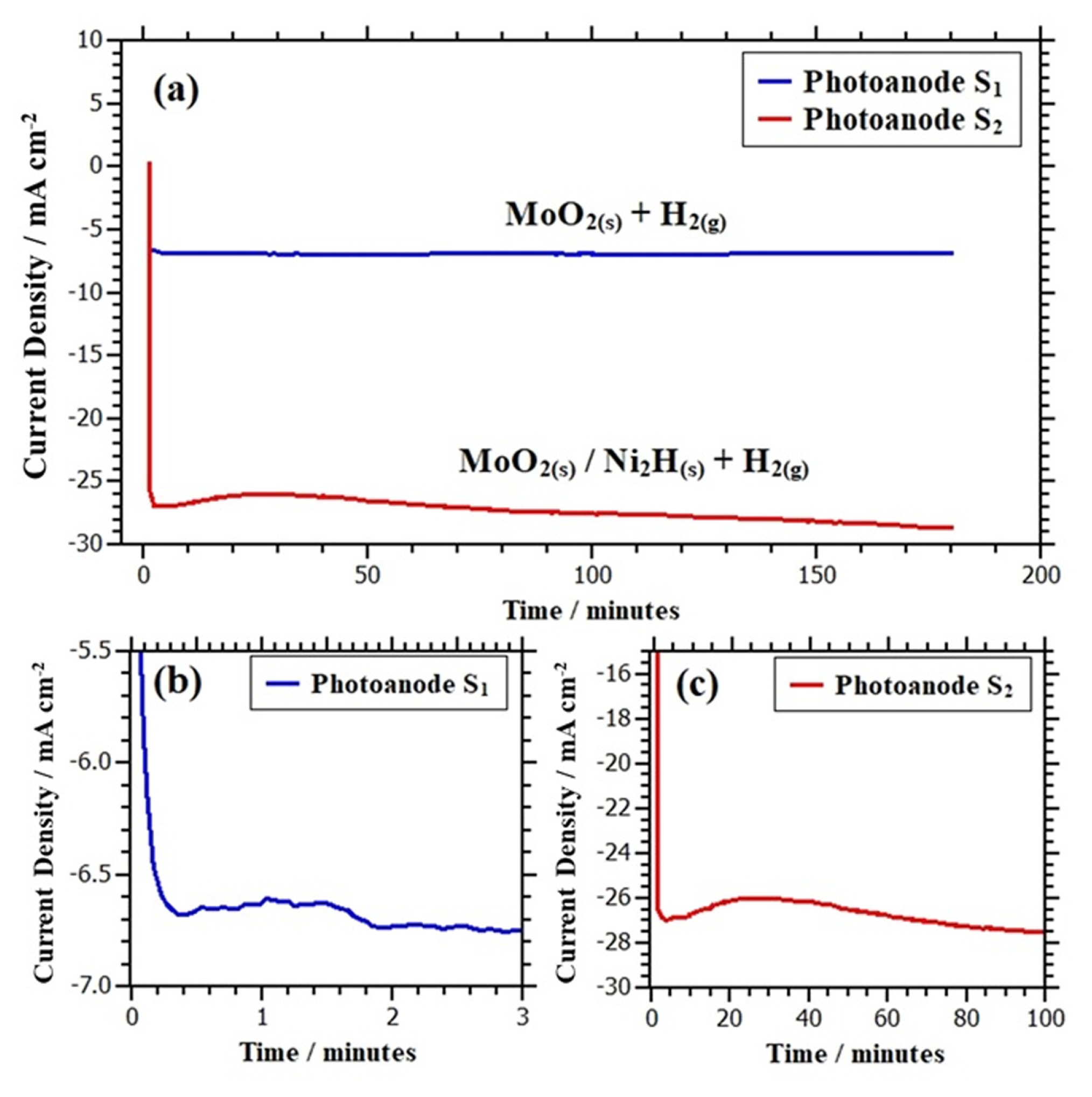
Fig. 2 depicts the curves of current densities as a function of time obtained in the electrodeposition experiments at a potential of ŌłÆ1.377 V vs. Ag/AgCl1) (3M) applied for 3 hours for the synthesis of photoanodes S1 and S2.
Fig. 2a shows that the cathodic current density curve obtained in the synthesis of photoanode S2 is larger than the cathodic current density curve obtained in the synthesis of photoanode S1 under the same experimental conditions. A zoom at the beginning of the current density curve of the photoanode S1 (Fig. 2b) reveals a small decrease in cathodic current density (< 2 min). This initial shape of the current density would be related to the formation of molybdenum oxides of the MoO2 type, which are probably partially blocking the electrode surface. The above would be caused because the high electronegativity of oxygen compared to hydrogen at room temperature (even in environments where there is a greater amount of hydrogen) would give greater stability to binary d-metal oxides, such as MoO2 instead of metal forms with lower states of oxidation as reported by Borgschulte et al. [25]. Studies carried out by Shembel et al. [26] confirm that at potentials lower than ŌłÆ0.68 V vs SHE the most stable species due to the reduction of molybdate ions, MoO42ŌłÆ is molybdenum dioxide, MoO2. This justifies the formation of molybdenum oxides instead of metallic molybdenum, even in the presence of hydrogen generated during HER.
Despite the current density curve obtained throughout the experiment would be a product of both the hydrogen evolution reaction and the reduction of molybdate ions to molybdenum dioxide, the steady-state value of the current density illustrated in Fig. 2a would correspond mainly to the HER as reported by Kuznetsov et al. [27-29]. Probably the high electrical conductivity2) of the MoO2 deposited on FTO-coated glass would have a positive impact on the HER since it would allow the passage of electrons easily from the substrate to the electrode | electrolyte interface promoting HER at the cathode surface.
Considering the above, the possible reactions that describe the reduction of molybdate ions to molybdenum oxide and the evolution of hydrogen during electrodeposition are the following:
On the other hand, Fig. 2c shows that for the photoanode S2 the current density has a concave shape during the first 70 minutes; this behavior could be attributed to two main factors:
Initial formation of the complex [NicitMoO2]ads [29].
Formation of the alloy MoO2(s)-Ni2H(s) from [NicitMoO2]ads.
The initial current density curve shape could be related to the partial blockage of the photoanode surface by an intermediate complex of the type [Nicit-MoO2]ads which would be formed under alkaline conditions at the working potential, as reported by Kuznetsov et al. [29]. The possible formation of the intermediate complex mentioned above would be given by the following [29]:
Afterward, the complex [NicitMoO2]ads gives rise to the formation of
[ Ni 2 ( OH ) 2 H 2 cit 2 ] ( aq . ) 4 -
Complex
[ Ni 2 ( OH ) 2 H 2 cit 2 ] ( aq . ) 4 -
In the next 110 minutes, the current density value continued to increase reaching approximately ŌłÆ29 mA cmŌłÆ2 at 180 minutes as illustrated in Fig. 2a. This current density had a more cathodic value than that presented by photoanode S1 during the same period. This behavior would be linked to the cathodic surface type. Chassaing [31] has reported that the nickel-molybdenum alloys are a good catalyst for the HER under similar experimental conditions (pH 9.5 and polarization range: from ŌłÆ1.3 to ŌłÆ1.6 V vs SSE) to those used in chronoamperometries made in this research. The above would explain the cathode current density increase in the last 110 minutes. This suggests that the MoO2(s)-Ni2H(s) alloy on the photoanode S2 surface would exhibit better electrical conductivity than the undoped molybdenum dioxide deposited on the photoanode S1 surface, promoting the HER on the cathode surface with ease, as shown in Fig. 2a.
3.2 Microstructural Analysis
In order to characterize the morphology of the undoped and nickel-doped molybdenum oxide films deposited on FTO-coated glass, the photoanodes S1 and S2 were analyzed by SEM and AFM.
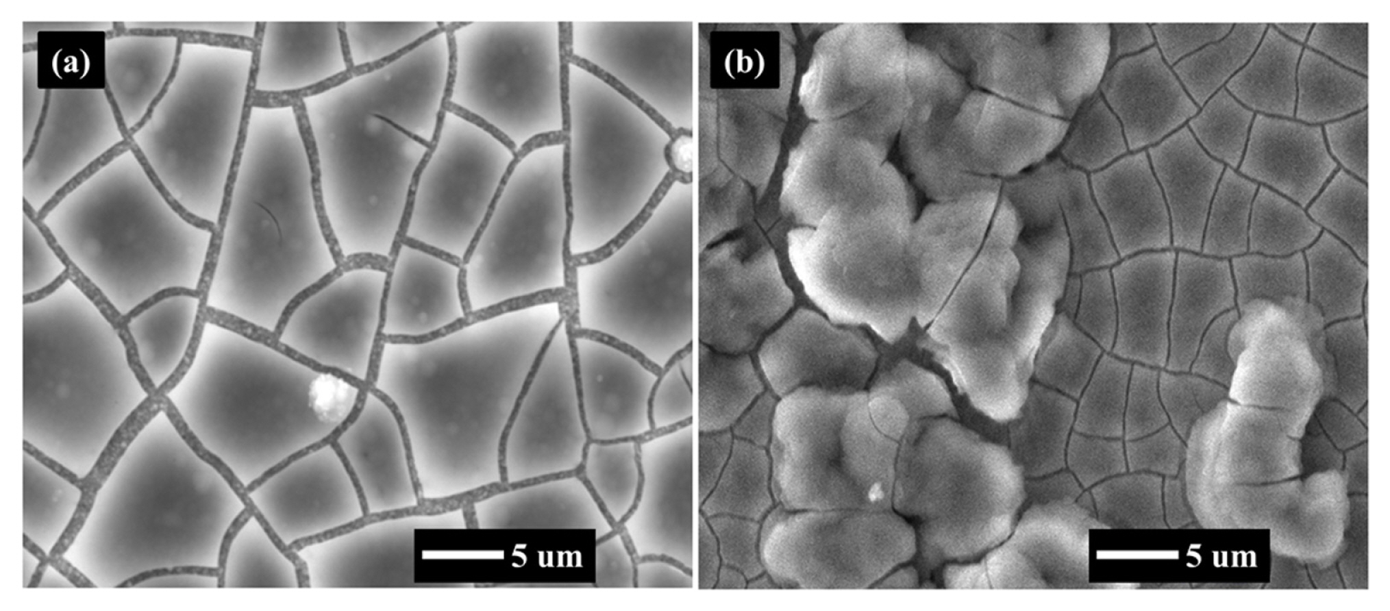
The surface morphology of the photoanodes was observed through SEM and the micrographs are presented in Fig. 3. According to this figure, SEM analysis revealed the presence of several cracks on the surface of the photoanodes S1 and S2. The loss of water from the deposited films on FTO-coated glass and the HER during the electrodeposition process is probably the main cause of the formation of cracks in these electrodes.
An SEM image of the photoanode S1 surface is shown in Fig. 3a. Unlike the photoanode S2 (Fig. 3b), it does not show the presence of irregularly shaped conglomerates. Indeed, it forms an orderly and homogeneous pattern over the entire surface of the photoanode S1. This comparison reveals the advantage of the MoO2(s)-Ni2H(s) alloy in the photoanode S2, since the conglomerates of irregular shape in this type of film would favor the PEC oxygen evolution reaction, due to the greater surface area and availability of active sites on it.
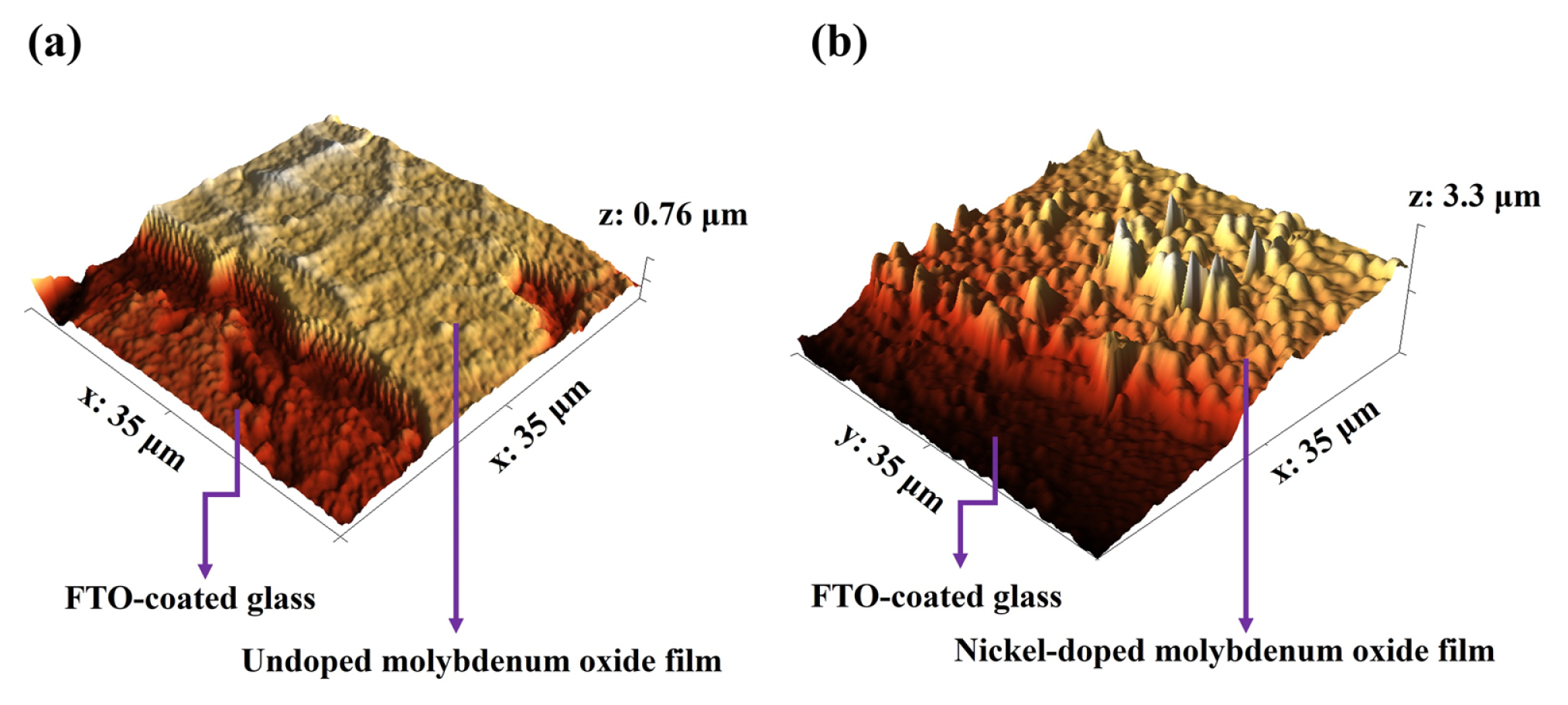
An AFM image of a nickel-doped molybdenum oxide film of the photoanode S2 is shown in Fig. 4b. According to this figure, MoO2(s)-Ni2H(s) films on the photoanode S2 surface exhibit an irregular morphology. Conglomerates and randomly located clusters are clearly observed on the film surface, which agrees with Fig. 3b obtained by SEM analysis of the photoanode S2. A surface examination revealed that these hill-like structures have an average width of 182 nm. The height of these conglomerates varied from 250 to 1,159 nm. Moreover, Fig. 4b shows that the film surface does not follow the pattern of the FTO-coated glass. In contrast to this, Fig. 4a corroborates that the photoanode S1 presents a film deposited without the presence of irregularly shaped conglomerates. The AFM image of the undoped molybdenum oxide film on the surface of the photoanode S1 presented in Fig. 4a, indicates the presence of a homogeneous film on the FTO-coated glass surface. Previously, thicknesses ranging between ca. 219 nm [15] and 1150 nm [13] have been reported for molybdenum oxide films obtained by electrodeposition. In this research, the thicknesses determined by AFM showed that the photoanode S2 presents a film3) on the substrate with an average thickness of 763 nm, while the photoanode S1 has a deposited film with an average thickness of 438 nm on FTO-coated glass, which is thinner than the film obtained on the substrate of the electrode S2. Both values are within the ranges reported in the literature [13,15]. For the photoanode S2, it is possible to assume that the nickel presence could modify the morphology and the thickness of the generated films. Indeed, Popczyk et al.[32] has reported that nickel-based coatings are among the most often used to obtain electrodes with a very developed, rough, thick, or porous electrode surface. This is due to the ease with which Ni2+ penetrates within interstitial spaces and besides the reaction of Ni with the basal (molybdenum) or lateral (oxygen) atoms of the metal oxide structure, modifying the morphology and properties of the semiconductor material [33].
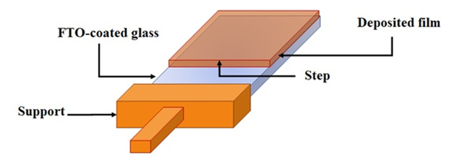
It is important to mention that to determine the thickness of the deposits in the AFM analysis, the step formed between the clean FTO-coated glass surface and the deposit was considered. The above is illustrated in Fig. 5.
3.3 Compositional Analysis
The composition and chemical state of the elements forming the films deposited on the surface of the photoanodes were characterized by EDS and XPS.
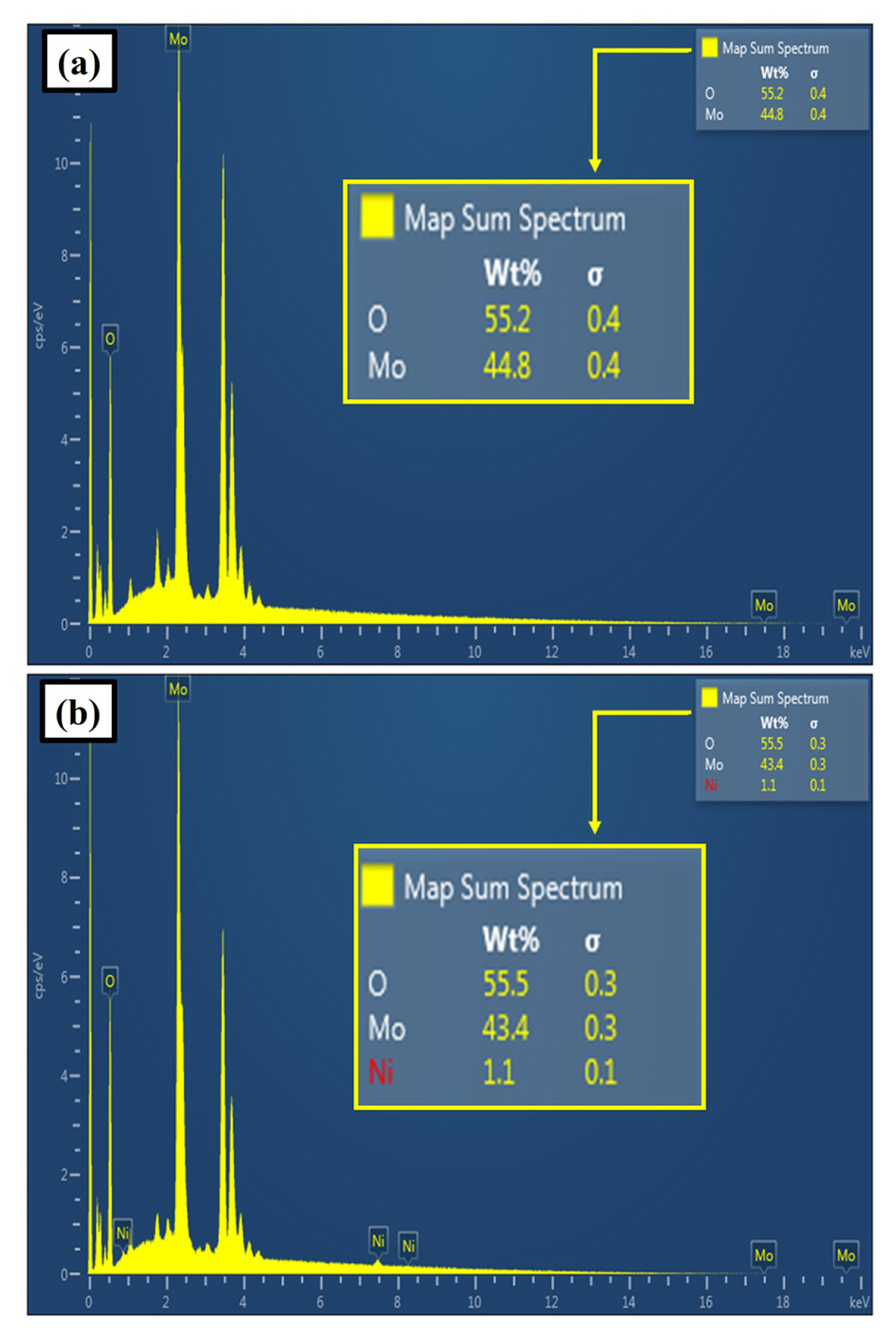
Figs. 6a and 6b show the EDS analyses for selected points (same micro-area used in the SEM analysis presented in Fig. 3) of the photoanodes S1 and S2.
The EDS spectra of the photoanodes S1 and S2 corroborate a strong presence of molybdenum (over 40 wt.% in both cases) in all the deposited films, which would be in the photoanodes mainly as MoO2 (as suggested by the XPS analysis) and MoO3 (formed from the partial oxidation of MoO2 in contact with the atmosphere).
The presence of oxygen at the photoanodes is also shown in the EDS spectra. The high amount of oxygen (over 55 wt.% in both cases) corroborates the presence of MoO2/MoO3.
For the case of the photoanode S2, as can be seen in Fig. 6b, it is possible to find nickel on the film surface of the photoanode S2 (1.1 wt.%), which would be mainly as Ni2H obtained from the electrodeposition and NiOOH obtained from the partial oxidation of nickel hydride in contact with the electrolyte during the electrodeposition.
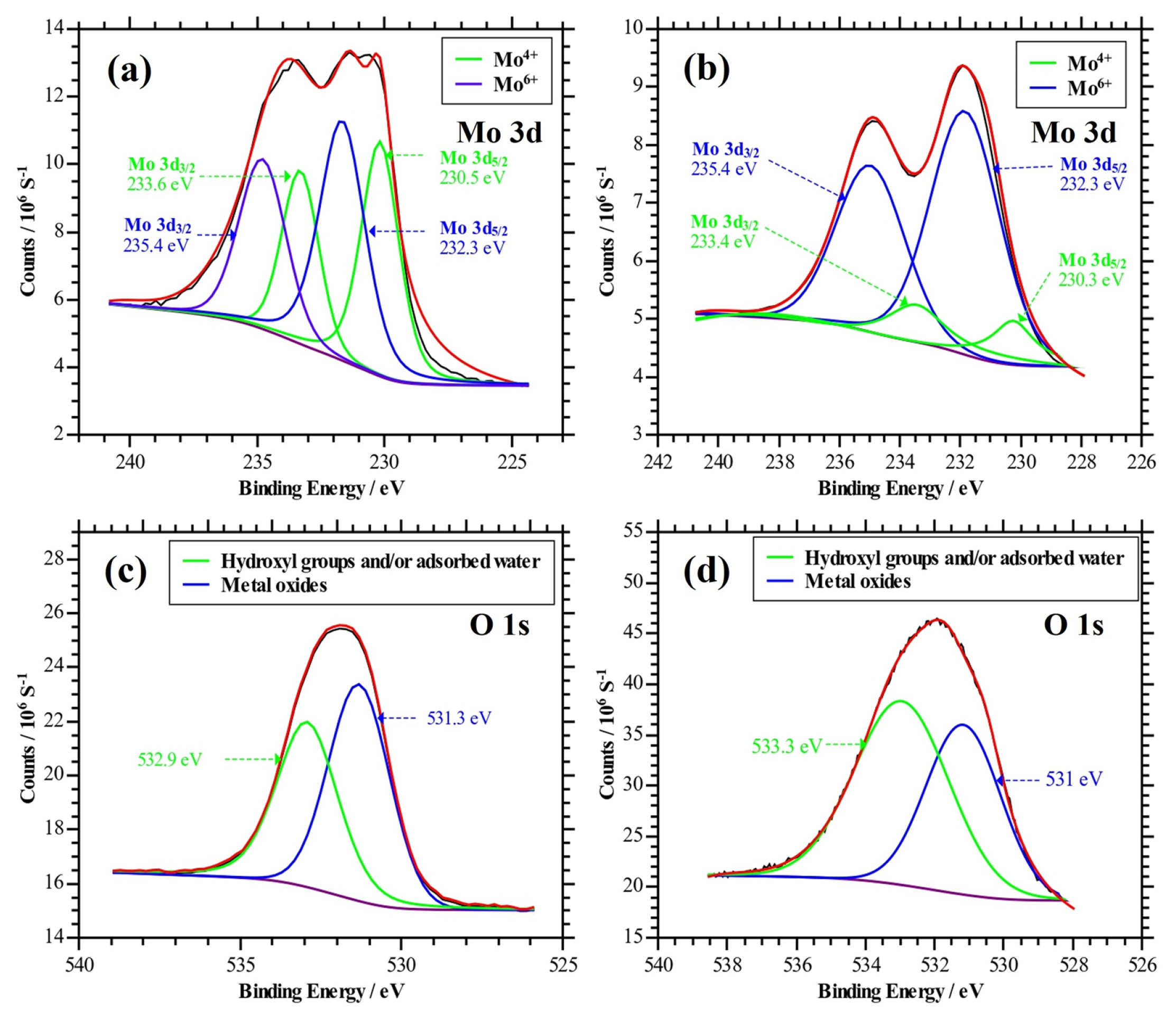
Figs. 7a and 7b show the Mo 3d XPS spectra for the photoanodes S1 and S2. As can be seen, the deposited films on the photoanodes contain the characteristic peaks of Mo4+ situated approximately at binding energies of 230 and 232 eV, attributed to the presence of MoO2 [34], which agrees with the reaction in Eq. (4) for both types of electrodes in section 3.1. However, at the same time, it is possible to see in all the films two characteristic peaks of Mo6+ situated approximately at binding energies of 232 and 235 eV, which would indicate the presence of MoO3 as well [34]. The presence of this type of oxide in the photoanodes would be explained by the exposure of the photoanodes to the atmosphere before the XPS analysis, which would lead to the surface oxidation of deposited films. Consistent with this research, Scanlon et al.[33] reported that for the peak Mo 3d, samples of MoO2 seemed to have an MoO3 surface layer when these samples were exposed to the atmosphere before XPS analysis and, therefore, it is likely that the data included components associated with changes in the sample induced by exposure to oxygen.
The O1s spectra for the films of the photoanodes S1 and S2 are shown in Figs. 7c and 7d. In all the films, it is possible to appreciate two peaks situated approximately at binding energies at 531 and 532 eV. In both photoanodes, the peaks at lower binding energies mainly correspond to metal oxides such as MoO2 and/or MoO3, whereas the peaks at higher binding energies correspond to hydroxyl groups or adsorbed water on the surface i.e. Mo-OH [35,36].
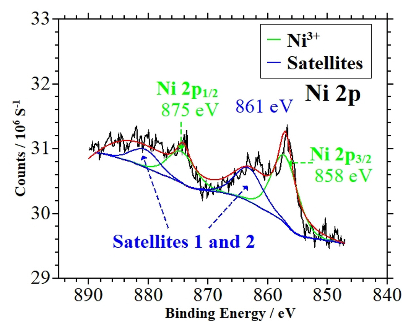
Fig. 8 illustrates the XPS spectra in the region of Ni 2p for the photoanode S2. For this sample, the Ni 2p exhibits a doublet Ni 2p1/2 and Ni 2p3/2. Analysis of the Ni 2p3/2 region shows the main component centered at 858 eV for the peak Ni3+. This peak is assignable to nickel oxyhydroxide (NiOOH) [37,38], which could be formed from the partial oxidation of the nickel hydride formed in the film (see section 3.1) due to the presence of water in the electrolyte. The above can be described by the following equation:
An additional peak at higher binding energy (centered at 861 eV) can be seen in Fig. 8, which could correspond to a satellite structure4) [37,38]. It is important to mention that the presence of satellite structures for nickel compounds with 0, +2, and +3 oxidation states is common at higher binding energies [37,38]. In fact, in the case of the photoanode S2, the correct assignment can be compromised by the complex mainline splitting due to multip contributions in oxyhydroxides and by satellite structures at higher binding energies, particularly in the most intense Ni 2p spectra where often the satellite structures are wide.
3.4 Optical Characterization
To have a complete optical characterization, analysis by UV-Visible spectroscopy and Tauc plots for the photoanodes S1 and S2 were performed.
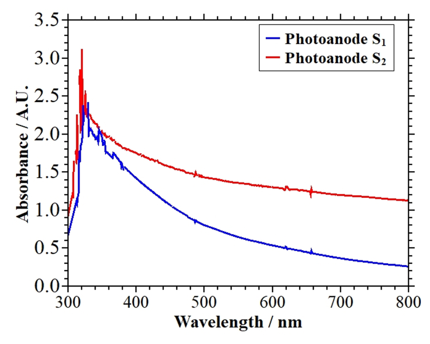
UV-Visible spectroscopy analysis was used to determine the absorbance of the photoanodes S1 and S2. Fig. 9 shows the absorption spectra of these photoanodes.
According to Fig. 9, the photoanodes S1 and S2 formed a similar pattern in the w range used in UV-Visible analysis. As can be seen, in these photoanodes, the absorption peak is reached at wavelengths below 400 nm. It is evident that the photoanode S2 had a greater absorption of light energy in the whole range of analyzed wavelengths, reaching its maximum in the UV region (the maximum absorbance of this electrode was ca. 3.1 at ╬╗ = 330 nm). As mentioned in section 3.2, this behavior can be attributed to the film morphology on the photoanode S2 surface. The presence of irregularly shaped conglomerates on the photoanode surface promotes large surface areas favoring the absorption of light energy [14].
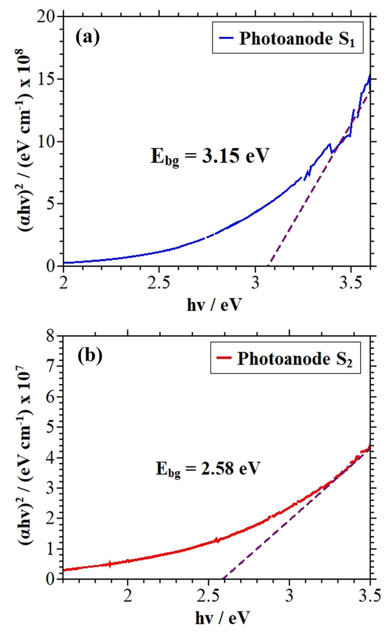
In solar energy conversion systems, the optical band-gap energy (Eg) of a semiconductor electrode is a key parameter. Only photons of equal or higher energy than the band-gap energy will be absorbed by the semiconductor film. The optical band-gap value of the deposited films was determined by the analysis of Tauc plots.
Tauc plots of photoanodes S1 and S2 are depicted in Figs. 10a and 10b. According to Fig. 10a, the photoanode S1 has a higher band-gap (ca. 3.15 eV) than the values obtained indirect transitions in other research [13,15] for electrodeposited molybdenum oxides in similar conditions to this research, which implies that this type of photoanode could present a greater resistance to the passage of electrons from the valence band to the conduction band of the molybdenum oxide deposited on the FTO-coated glass. Semiconductor materialsŌĆÖ large band-gap as in the case of the photoanode S1 results in a reduced use of the solar spectrum [39]. On the other hand, the photoanode S2 (Fig. 10b) exhibits a band energy value of 2.58 eV, which could be attributed to the incorporation of Ni3+ in the MoO2/MoO3 structures, contributing to the formation of a shallow donor energy level below of the conduction band of the molybdenum oxide.
3.5 Photoelectrochemical Characterization
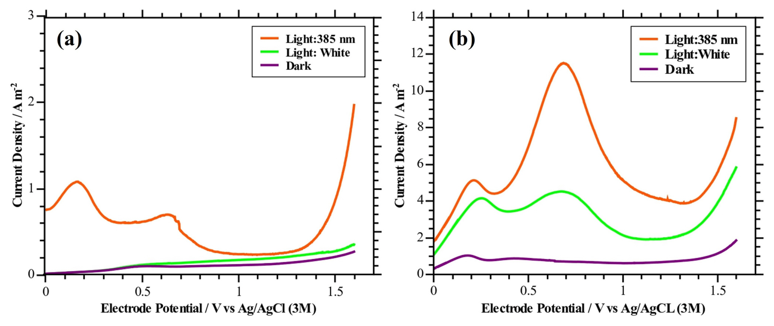
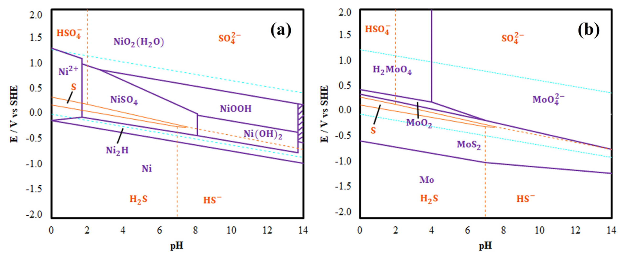
Representative linear sweep voltammograms of the photoanodes S1 and S2 obtained in an electrolyte of Na2SO4 0.1 M at pH 3.5 are presented in Figs. 11a and 11b. Additionally, in order to obtain a better understanding of the phenomena in the system in which the photoelectrochemical experiments were carried out, Eh-pH for the nickel and molybdenum species have been elaborated. Figs. 12a and 12b show the obtained which will be used to interpret and describe the processes that occur during the LSVs.
The analysis of the LSV (Fig. 11b) for the photoanode S2 shows two peaks centered at 0.2 V (ca. 0.4 V vs SHE) and 0.75 V (ca. 0.95 V vs SHE) when the photoanode is illuminated (white light and UV light). These peaks could be associated to the redox transition of Mo4+ to Mo6+. Likely, in the acidic electrolyte used in this voltammetry, the formation of H2MoO4(aq.) from the MoO2(s) present in the photoanode surface begins at this potential range according to the following reaction mechanism:
The above agrees with the information provided by the Eh-Ph diagram in Fig. 12b, where it is possible to appreciate that at the indicated pH and potential range, the formation of H2MoO4(aq.) from the MoO2(s) is favored. On the other hand, the second peak also could be caused by the formation of NiO2(H2O)(s) from NiOOH(s) present in the film surface, according to the Eh-pH diagram in Fig. 12a. The formation of NiO2(H2O)(s) is given by the following reaction:
As can be seen in the voltammogram in Fig. 11b, when the photoanode is illuminated under UV and white light there is an increase in the current density curves from ca. 1.3 V (ca. 1.5 V vs SHE) that would correspond mainly to the PEC oxygen evolution reaction present at the anode surface, which is to be expected in that potential zone. On the other hand, in the LSV under dark polarization conditions of the photoanode S2, the presence of a small peak around 0.2 V can be observed. This peak shows that the MoO2(s) present in the deposited film could be giving way to H2MoO4(aq.) formation under the experimental conditions, which would indicate a possible instability of the deposited film. The current increase at 1.4 V under darkness is related to the electrochemical oxidation of water molecules.
About the photoanode S1, it is possible to see that under ultraviolet illumination the current density curve (Fig. 11a) presents similar peaks to the voltammograms obtained for the photoanode S2 under light conditions. This suggests that the formation of H2MoO4(aq.) is present during the study performed by voltammetry in this electrode. When the voltammetries are performed with white light or in dark conditions, the presence of a small peak around 0.5 V (ca. 0.8 V vs SHE) can be observed. This peak indicates that the MoO2(s) present in the deposited film may not be fully stable. In the case of this photoanode, an increase in the current density curve under UV illumination can also be observed from ca. 1.4 V (ca. 1.6 V vs SHE) which correspond to the PEC oxygen evolution reaction present at the anode surface.
4. Conclusions
Photoanodes S1 and S2 were synthesized through electrodeposition. From these experiments, it was determined that the MoO2 is the species formed on the undoped molybdenum oxide electrode surface (photoanode S1), while the MoO2-Ni2H alloy would form the nickel-doped molybdenum oxide film (photoanode S2).
The microstructure of the photoanodes was analyzed using SEM and AFM techniques. From these analyses, it was determined that, unlike the morphology of the undoped molybdenum oxide film present on the photoanode S1 which forms an ordered and homogeneous pattern over the entire surface of the electrode, the morphology of the nickel-doped molybdenum oxide film present on the photoanode S2 is heterogeneous. and irregular with hill-like conglomerates of random orientation on top of the substrate. In addition, the doped film has an average thickness of 763 nm, while the photoanode S1 has a deposited film with an average thickness of 438 nm. All this suggests that nickel doping had a significant impact on the morphology type and the deposited film thickness.
The composition and chemical state of the elements forming the films were characterized by XPS and EDS. It was concluded that the photoanodes surface was partially modified (oxidized) due to the interaction with the atmosphere and the electrolyte during the electrodeposition. It was revealed by XPS that MoO3 and NiOOH are present as a result of partial oxidation of the MoO2-Ni2H alloy in the photoanode S2, while MoO3 was detected on the photoanode S1 product of the partial oxidation of MoO2 on the electrode surface. On the other hand, EDS analysis shows in all the photoanodes the presence of Mo (over 40 wt.%) and O (over 55 wt.%), which confirms that the films are composed of molybdenum oxides. Moreover, nickel in small quantities (1.1 wt.%) was found on the photoanode S2 surface, which would be mainly as Ni2H obtained from the electrodeposition and NiOOH obtained from the partial oxidation of nickel hydride in contact with the electrolyte during the electrodeposition process.
The photoanodes S1 and S2 absorb UV and blue light (ca. wavelengths from 300 to 500 nm) and present a direct (allowed transitions) band-gap. Tauc plots showed that the photoanode S2 had the lowest optical band-gap energy value (2.58 eV) compared to the photoanode S1 (3.15 eV), which results in better use of the solar spectrum.
The photoelectrochemical analyzes indicate that the photoanodes S1 and S2 present photoactivity, reaching their maximum under UV illumination. This is consistent with the optical characterization of these photoanodes. In general, nickel doping of the photoanode S2 resulted in a higher photocurrent in all case studies in the LSVs, which would corroborate that nickel doping favored a better photoactivity of these electrodes. Nevertheless, both types of electrodes could present some degree of instability in the experimental conditions.
The obtained results are satisfactory and show that the produced photoanodes present interesting semi-conducting and catalytic properties for their application in an electrochemical cell for water splitting, although their stability must be improved. Consequently, to obtain chemically stable photoanodes, future work should focus on finding a suitable electrolyte and appropriate experimental conditions (potential, pH, or post-calcination treatment). In the case of molybdenum oxide photoanodes, it has been reported [15] that for water splitting applications, these films would need a post-calcination treatment to obtain stable photoanodes. It is suggested to avoid contact with acid solutions of these photoanodes since it favors the degradation of deposited films.