


1. Introduction
Silicon surface has attracted considerable attention because it shows unique physical properties when it is modified [1,2]. The modified silicon surface has been used as the functional surfaces for various applications such as photoelectrochemical hydrogen production [3,4], sensors [5,6], photoluminescence [7ŌĆō9], electroluminescence [10], solar cell [11], and lithium ion battery [12,13]. These properties result from the nanostructure of the silicon surface [3]. For example, photoluminescence is well-known to result from the quantum size effects observed from the small dimensions (~5 nm) of the free exciton of bulk Si [14]. The nanostructure of the silicon surface can be easily achieved by the etching method [15].
In our group, we have investigated the etching reactions of Si(111) surface in fluoride solutions. We reported that the triangular pits play an important role on the preparation of a ultraclean Si(111)-H surface [16] and that the etching reactions are strongly dependent on the pH of the etching solution [17] and the applied potentials [18].
Here, we investigated the chemical and electrochemical etching of Si(111) surface in a dilute fluoride solution by using electrochemical and electrochemical-scanning tunneling microscopic (EC-STM) techniques. Previously, we studied the electrochemical etching reactions of the Si(111) surface from cathodic to slightly anodic potential regions [17,18]. In this work, we performed the EC-STM measurements on the Si(111) surface electrochemically treated at far anodic potential region where a porous nanostructure can be formed on the silicon surface. For the silicon surface etching, aqueous solutions of HF, NH4F, and NaOH, and water itself have been used. Among these, water is too weak to prepare the porous nanostructure [19]. HF is one of the most dangerous reagents in terms of handling in a laboratory; it involves vigorous vapor evolution during electrochemical etching, which is dangerous as well. Concentrated NH4F, e.g. 40 wt.% NH4F [20], and NaOH solutions [21] are too strong etchants to preserve the porous structure on the silicon surface. Therefore, we chose 0.2 M NH4F aqueous solution (pH 5.0) as the electrolyte herein because it is relatively less dangerous and the slightly acidic environment allows activation of the silicon surface by a hydroxide ion, which is well known as the main etchant for silicon [21,22]. The obtained results provide information on the preparation of nanostructure on the Si(111) surface by chemical and electrochemical etching [15,23].
2. Experimental
Silicon (111) wafers (n-type, 1ŌĆō12 ╬®cm, <0.5┬░ miscut) were cleaned in a sonication bath of Milli-Q water (resistivity > 18 M╬®cm) and acetone, oxidized in a H2O2:H2SO4 (1:3) solution for 20 min, rinsed with Milli-Q water, and finally dried under flowing purified nitrogen gas.
Electrochemical measurements were performed under a standard electrochemical condition, with two platinum wires as counter and reference electrodes, under a nitrogen atmosphere at room temperature. In this work, we measured the potential difference between the Pt pseudo-electrode and saturated calomel electrode (SCE) in the etching solution and all potentials are quoted versus SCE for the convenience. After the electrochemical treatments, the samples were rinsed thoroughly twice with Milli-Q water, and 0.1 M H2SO4 was poured into the cell, followed by the quick application at a potential negative than open circuit potential (OCP). The EC-STM measurements were carried out using PicoSPM and PicoStat (Molecular Imaging Corp.). STM tips were made from an 80:20 Pi-Ir wire (0.2 mm in diameter) by mechanical cutting, and then were coated with a nail polish to reduce the area in contact with the electrolyte. Solutions were prepared with Milli-Q water. All solutions and chambers used in this study were purged with Ar or N2. The pH of 0.2 M NH4F solutions was adjusted by adding 0.2 M HF to preserve the fluoride concentration constant.
3. Results and Discussion
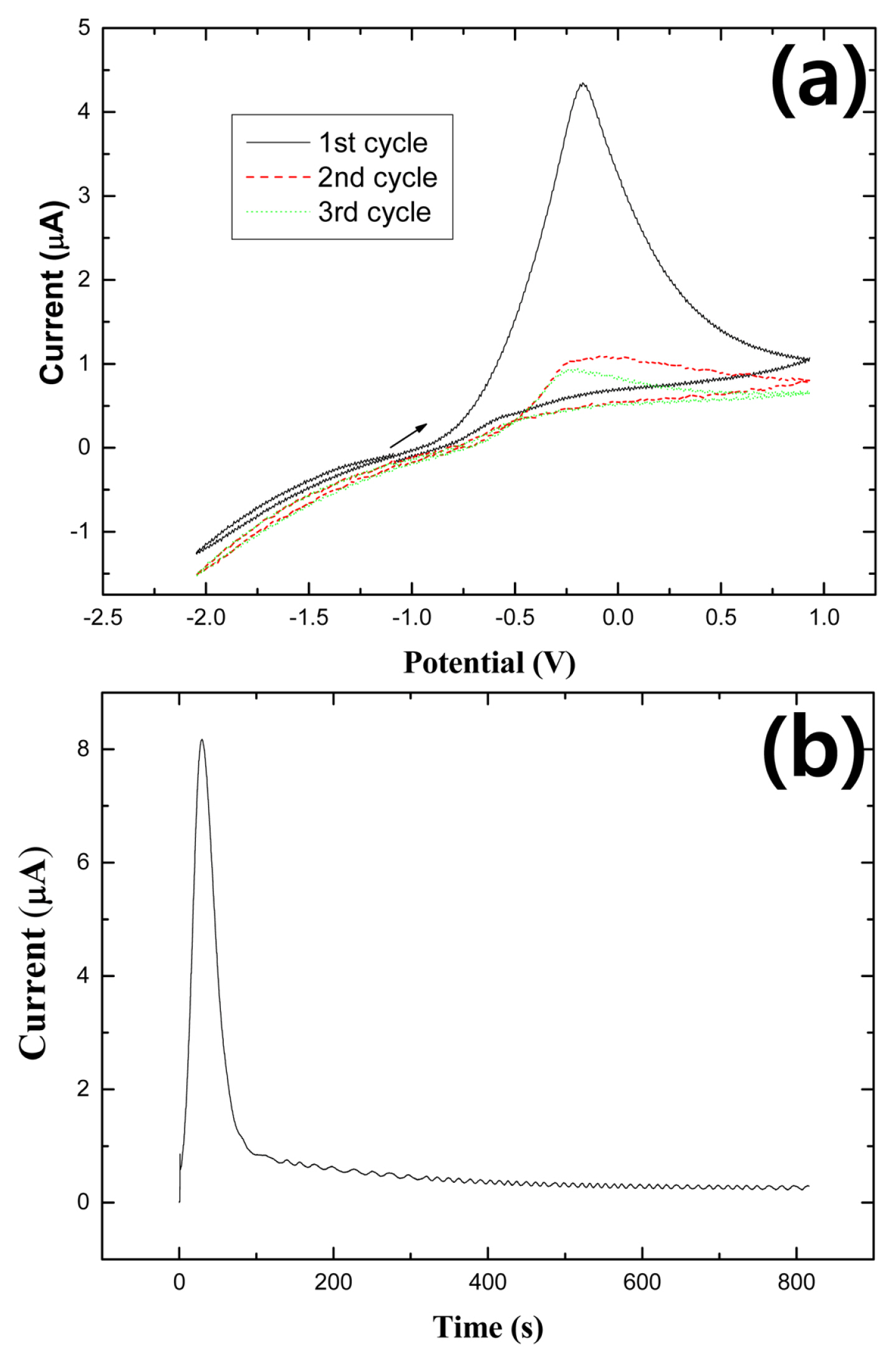
Fig. 1a shows cyclic voltammograms of n-Si(111) oxide obtained in deoxygenated 0.2 M NH4F (pH 5.0) in the potential region between ŌłÆ2.0 V and +1.0 V at a scan rate of 25 mV/s. In the first cycle, current appeared almost zero until ŌłÆ0.8 V, abruptly increased at ŌłÆ0.7 V, peaked at ŌłÆ0.2 V, and decreased sequentially. In a cathodic sweep, only the hydrogen evolution reaction occurred on the Si(111)-H surface. The abrupt increase of current in an anodic range indicates that the Si(111) oxide layer was anodically stripped [16,18]. Here, the stripping of the Si(111) oxide may take place through two steps, chemical and electrochemical reactions. Firstly, the thick oxide layer is chemically removed by HF and then, the interface between the oxide layer and Si(111) bulk undergo the anodic reaction [24]. The anodic peak current at ŌłÆ0.2 V is, therefore, attributed to the stripping of Si(111) oxide layers with the injection of an electron to the conduction band of the n-Si(111) electrode [25,26]. The cathodic current in the second cycle negatively increased slightly because the stripping of the Si(111) oxide layer in the first cycle made the Si(111) surface electroactive. Unlike the cathodic current, anodic current considerably decreased in the second cycle, suggesting that the Si(111) oxide layer was almost stripped in the first cycle. In the third cycle, the current was very similar to that of the second cycle. The cyclic voltammograms are well consistent with those in the literature [27].
Fig. 1b shows a current transition curve of the oxide-covered Si(111) from OCP to +0.5 V in 0.2 M NH4F of pH 5.0. The current showed an initial small spike, suddenly increased and decreased, and then continuously decreased to 1 mA/cm2 for 800 s. This trend agrees with the result reported by the Lewerenz group [24]. In their report, it was explained that such a low current around 800 s is due to the perfectly hydrogen-terminated and clean Si(111) 1├Ś1-H surface.
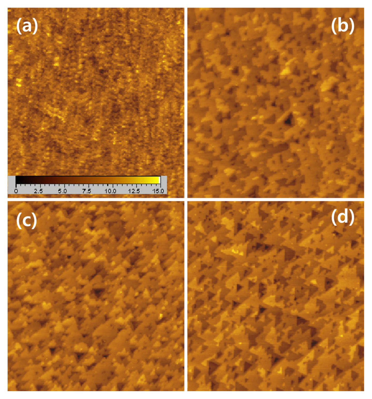
Fig. 2 shows EC-STM images of the Si(111) surface obtained in 0.1 M sulfuric acid after treatments of the thin oxide-covered Si(111) sample at OCP in 0.2 M NH4F solution of pH 5. The first image (Fig. 2a) was taken after chemical etching for 350 s. The surface was distributed with small round particles that could be silicon oxides. After the etching of the silicon surface for 470 s (Fig. 2b), the surface morphology changed, that is, the round islands were still randomly distributed and atomically flat surfaces and triangular pits started to appear, which represents the interface of the silicon/silicon oxide layer. After 530 s etching of the silicon surface (Fig. 2c), the edges of the terraces and triangular pits became straight. However, many edges of the terraces were still rounded. The 700 s etching (Fig. 2d) removed the entire oxide layer and made most of the steps straight and sawlike, indicating that the di- and tri-hydrides at kink and step sites were etched more rapidly rather than those on the terrace, at which straight edges with [112̄] oriented steps of the stable monohydrides remained. As a result, the etching of the Si(111)-H in the fluoride solution of pH 5 made the surface atomically rough with many triangular pits.
EC-STM images of the Si(111) surface obtained in 0.1 M sulfuric acid after electrochemical treatments of the thin oxide-covered Si(111) sample at ŌłÆ1.0 V in 0.2 M NH4F solution of pH 5 are presented in Fig. 1S of a supporting information. At ŌłÆ1.0 V, which is far negative potential against the flat band potential (FBP; ŌłÆ0.4 V) of the silicon [28], almost twice etching time (850 s in Fig. 1Sb) was needed to strip the oxide layer than that at the OCP. After the stripping of the oxide layer (Fig. 1Sc), the step edges neither evolved further nor became straight. The etching behavior of the surface is due to the cathodic stop of the etching reactions of the Si(111)-H surface previously reported by our group [18].
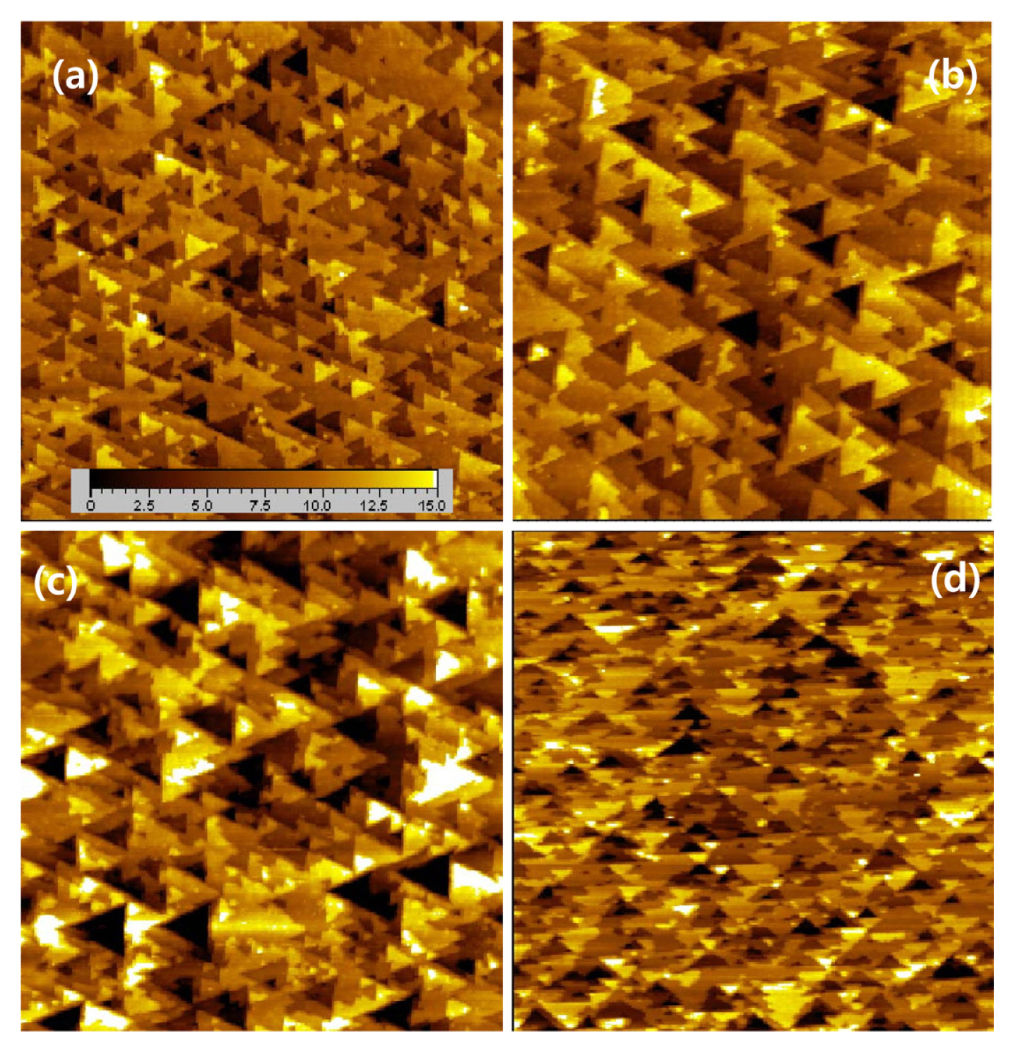
The EC-STM images of Si(111) surfaces treated for 700 s near the FBP and at the potentials more positive than the FBP are displayed in Fig. 3. The EC-STM images obtained after the electrochemical etching of the Si(111)-H surfaces for various times are shown in Fig. 2SŌĆō5S of the supporting information. The EC-STM image of the Si(111)-H surface treated at the FBP (Fig. 3a) shows the surface morphology similar to that at the OCP (Fig. 2d). The images of the Si(111) surface treated anodically (Fig. 3b, c, and d) were much different from those obtained at the FBP and the potential more negative than the FBP. As the applied potential increased, the triangular pits became larger and deeper. It is clearly shown that the triangular pyramids and deep pits were conspicuously formed on the Si(111)-H surface at +0.5 V (Fig. 3c). However, the electrochemical treatment at +1.0 showed a slightly different trend. As shown in Fig. 3d, the population of the triangular pits considerably increased. The height variation of the triangular structures was less severe (note white color in the image) and their sizes were smaller than those etched at +0.5 V.
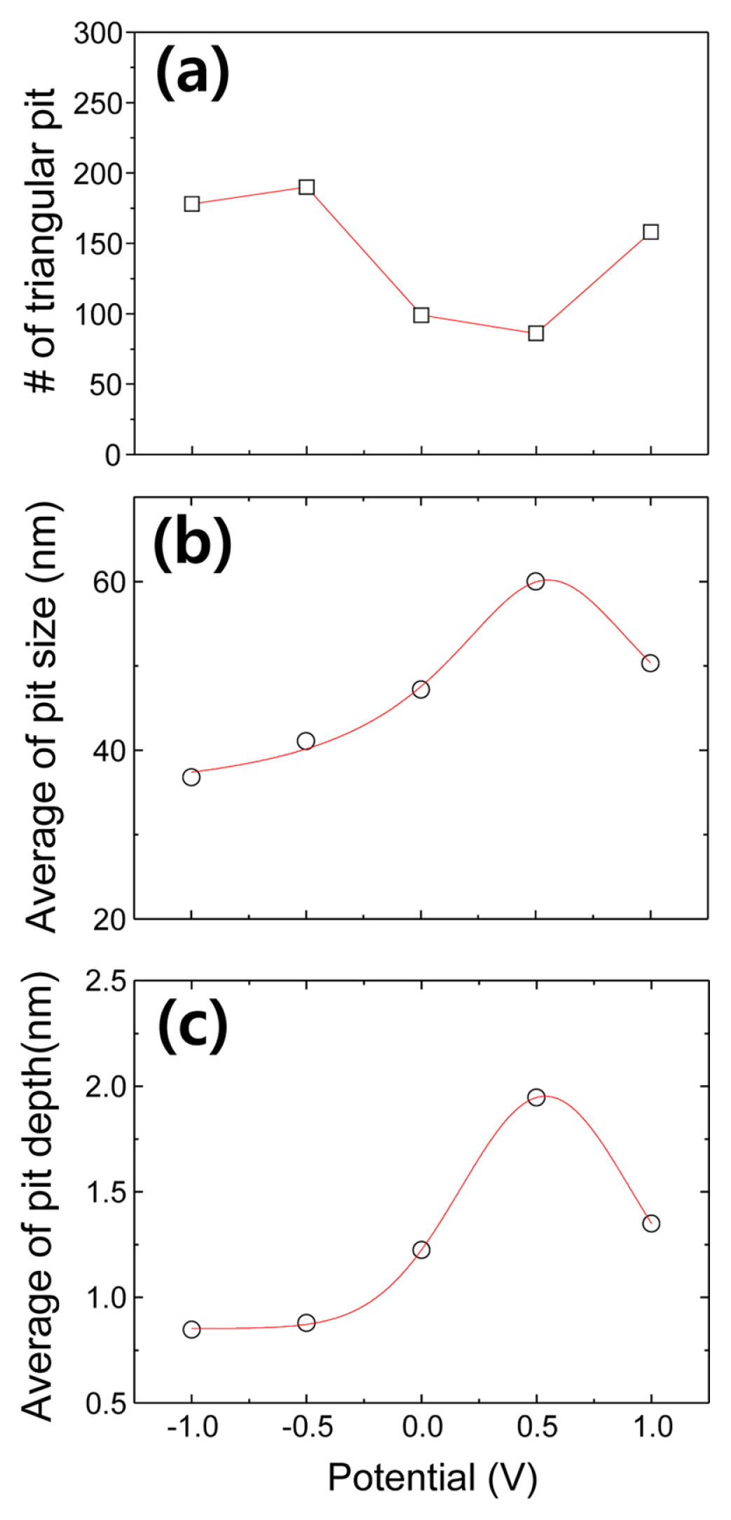
It is difficult to directly extract the information about the dependences of potential and etching time of the Si(111) surface from EC-STM images. Therefore, to statistically investigate the etching reaction of the Si(111) surface, we analyzed the pit number and structures such as pit size and depth in the EC-STM images. Fig. 4 shows the potential dependence of the evolution of the triangular pits in the EC-STM images. Fig. 4a exhibits the number of the triangular pits formed on the Si(111) surface after 700 s of electrochemical etching. The number of the triangular pits on the Si(111)-H surface treated at the potentials negative than the FBP was about 180. As the potential increased, it slightly decreased up to +0.5 V and then increased at +1.0 V. Large number of the triangular pits on the Si(111) surface electrochemically treated at the potential negative than the FBP may reflect that the structure exists at the interface between bulk Si(111) and a silicon oxide layer because the surface reaction of Si(111)-H almost stopped at the cathodic potential after the oxide layer was stripped [18]. As the potential increased to the FBP or slightly more than the FBP, the pit number decreased. This trend may be due to the step flow reactions that enlarged the triangular pits without the formation of new pits on the terraces. Therefore, the enlarged triangular pits were united with one another by the reactions and then gradually disappeared. At +1.0 V, the pit number increased conspicuously, indicating that the nucleation of the new pits on the Si(111) terraces occurred at the high anodic potential. Fig. 4b and 4c show the potential dependences of the triangular pit size and depth, respectively. For these graphs, we chose ten largest pits in each EC-STM image, measured their size and depth, and then averaged them. The pit size continuously increased from ŌłÆ1.0 V to +0.5 V and abruptly decreased at +1.0 V. The increment of the pit size to +0.5 V could result from the enhancement of the step flow reaction rate proportional to the applied potential [18]. Interestingly, the pit size became smaller at +1.0 V than that at a lower potential. The step flow reaction rate is extremely higher than ~100 nm/min at such a high anodic potential [18]. Here, we used the Si(111) wafer with a miscut angle, 0.5┬░, whose terrace width is expected to be as wide as ~50 nm [29]. Therefore, the highest layer of the 50 nm wide terraces can quickly disappear on the Si(111) surface. The depth of the triangular pits was almost constant at the potentials more negative than the FBP in Fig. 4c. It suddenly started increasing at the potential more positive than the FBP and then decreased at +1.0 V. These results indicate that the nucleation of the new pit was initiated at the potential more positive than the FBP. However, the pit number did not increase even at 0.0 V and +0.5 V in Fig. 4a, suggesting that the new pit formation was restricted inside the pits at the potentials. Based on the information on the anodic etching reaction at +1.0 V in Fig. 3 and 4, and literature [18], we can confirm that the pits were nucleated on the entire Si(111)-H surface and that the step edges are simultaneously eroded quickly at the high potential. Therefore, the step flow reaction at +1.0 V was too fast for the size and depth of the pits to grow, as shown in Fig. 4b and 4c.
The results presented here provide considerable insight regarding the electrochemical reactions of the Si(111)-H surface in a fluoride solution. In particular, the results indicate the etching condition for the porous nanostructures of the Si(111) surface. According to the EC-STM images, the anodic etching reaction, step flow reaction, occurs at the potential more positive than the FBP. The nucleation reaction of the pore, here pit, also occurs at the anodic potential. However, the nucleation reaction of the pit is restricted inside the pore at the potentials between the FBP and +0.5 V. At +1.0 V, the nucleation of the pits not only vigorously occurred on the entire surface of the Si(111) surface but the triangular pits also disappeared fast, i.e., the electropolishing reaction, so that the pits could not be deepened further. These results are consistent with the one reported by OzanamŌĆÖs group [30]. They reported that the electropolishing reaction occurred at a potential more positive than +0.3 V, while the porous Si layer was formed between 0 V and +0.3 V. They used 0.05 M HF as the etchant in 1 M HCl (pH 0). This difference in pH and fluoride concentration between our study and OzanamŌĆÖs could induce a slight shift of the reaction potential in the etching reaction. Therefore, we can conclude that the potential between the FBP and about +0.5 V as the anodic potential is appropriate to prepare a porous nanostructure on the Si(111) surface in the 0.2 M NH4F solution.
4. Conclusions
Electrochemical and electrochemical-scanning tunneling microscopic techniques were employed to study the evolution of surface morphology during the electrochemical etching of Si(111)-H in 0.2 M NH4F solution of pH 5. In a case of electrochemically anodic etching, the low anodic dark current indicated that the hydride was terminated on the Si(111) surface, which was followed by the formation of the triangular-shape structure with stable monohydride terminated edges through the step flow reaction. At the anodic potentials below +0.5 V, the nucleation reaction of the pit inside the triangular pits was superior to the step flow reaction. On the contrary, at +1.0 V, the electrochemical polishing reaction dominated. Therefore, it is suggested that a potential ~+0.5 V is appropriate to prepare the porous nanostructure on the Si(111) surface.