Growing High-Quality Ir-Sb Nanostructures by Controlled Electrochemical Deposition
Article information
Abstract
The electrochemical preparation and spectroscopic characterisation of iridium-antimony (Ir-Sb) species is important owing to their potential applications as nanostructure materials. Nanostructures, i.e. nanoflower and nanodisk, of Ir-Sb were electrodeposited on conductive substrates using a practical electrochemical method based on the simultaneous underpotential deposition (UPD) of Ir and Sb from the IrCl3 and Sb2O3 at a constant potential. Electrochemical UPD mechanism of Ir-Sb was studied using cyclic voltammetry and potential-controlled electrochemical deposition techniques. Herein, X-ray diffraction, scanning electron microscopy, energy dispersive spectroscopy, X-ray photoelectron and Raman spectroscopy were used to determine the morphological and structural properties of the electrochemically-synthesised Ir-Sb nanostructures.
1. Introduction
Recently, thermoelectric materials have attracted considerable research attention for converting heat energy directly into electrical energy or vice versa to enable the use of electrical energy with high efficiency in cooling systems [1]. Skutterudite compounds with a general formula of TX3, where T = Co, Rh and Ir and X = P and Sb, are the thermoelectric materials, such as CoSb3, IrP3, IrAs3 and IrSb3, with a narrow bandwidth, showing enhanced electrical and magnetic properties [2–4]. However, there is not enough information on the physical properties of binary skutterudite compounds. These semiconductors have a wide range of applications from cooling systems and generators to space technologies [5]. Particularly, V–VI semiconductors are the best known thermoelectric materials at room temperature. Thermoelectric materials have attracted considerable attention owing to their high reliability, low maintenance, long life and non-emission of toxic gas. For example, when Bi2Te3/Sb2Te3-based materials [6] are synthesised at nanoscales, such as superlattice structure [7], nanofilm [8], nanorod [9] and nanowire [10], they become Bi2Te3/Sb2Te3 quantum-well superlattice structures owing to their size limitations [11]. Excellent properties, such as adjustable physical, optical, electrical and thermoelectric properties, can be achieved at the nanoscale by changing both the size and composition of binary compound semiconductors [12].
Currently, several methods, such as chemical vapour deposition, chemical bath deposition, molecular-beam epitaxy, atomic layer epitaxy (ALE) and electrochemical deposition method, are used to synthesise nanoscale semiconductor materials that have revolutionary potential owing to their surface morphology peculiar to the nanoscale. Among these techniques, electrochemical deposition method has the advantages of magnifying nanostructures in a controlled manner and is an economical, fast and simple method for the preparation of large area thin films [13]. Surface morphology and growth rates are easily controlled by reactive, current density, deposition potentials added to salt concentration [14] Although the electrochemical deposition technique [15] has the advantages of being controlled at an atomic level and determining film thickness by the number of cycles, it has the disadvantages, such as the need for electrode washing process, which causes potential loss, reproducibility problem of the deposit and waste of time and solution.
To overcome these deposition problems, a single solution containing both species should be used, and deposition should be made at a single potential and UPD should be employed. UPD is defined as the electrochemical deposition of metal ions on the surface of substrate at a potential more positive than the Nernst potential for the electrodeposition of metal [15,16]. The UPD technique, i.e. restricted surface reaction, appears promising for the production of nanostructured materials that have controllable morphology potential and high purity. The first UPD-based electrochemical deposition method developed by Stickney is the electrochemical ALE [17] method based on the consecutive UPD of different elements [18–20] Recently, a UPD-based codeposition method has been developed to conduct the electrodeposition of composite semiconductor from the same solution at a common UPD potential [21,22] and has been successfully used in the formation of nanostructured compound semiconductors by other scientists [23,24]. If the deposition during the synthesis of semiconductor compounds is done at a UPD potential suitable for both species from the solution that contains the compounds forming the film, it can be asserted that the films obtained would be of higher quality and the synthesis can be continued up to the desired thickness by controlling the deposition duration.
From this viewpoint, the synthesis Ir-Sb thin films with excellent structures by electrodeposition method and determining the morphological and structural properties by various characterisation methods have been done. Herein, prior to the electrodeposition of each compound semiconductor, appropriate conditions, solution behaviours and concentrations have been determined, and electrochemical conditions have been examined for each component within these semiconductors. Potential semiconductor deposition has been performed using a potential-controlled electrolysis technique at a potential value for each species selected using the cyclic voltammetry technique in the UPD regions. As shown in Scheme 1, the general experimental strategy employed in this study involved controlled sizes and then performing electrochemical deposition of Ir-Sb.
The aim of this work is possible to grow highly crystalline deposits of Ir-Sb by a electrochemical method. Understanding of this upd process requires better knowledge of the mechanisms of basic such as the formation of two dimensional layers of Ir-Sb. The amount of Ir-Sb deposits of the thin films can be controlled by variation electrochemical deposition time. The time-varying film thickness and variations in the optical properties of these compound semiconductors have been then determined using the UV-vis technique. The morphologies of the obtained structures have been analysed using SEM and AFM techniques to observe their change with time along with the nucleation and growth stages and the change in the crystal structure of the films by time. Their characteristic tendencies have been analysed using XRD technique and their stoichiometry, i.e. the ratio of different elements in the films, has been analysed using EDS technique. XPS and Raman techniques have been used to obtain more detailed information about the type of surface compounds and structures of Ir-Sb films for which a qualitative analysis has been conducted using EDS technique to a certain degree.
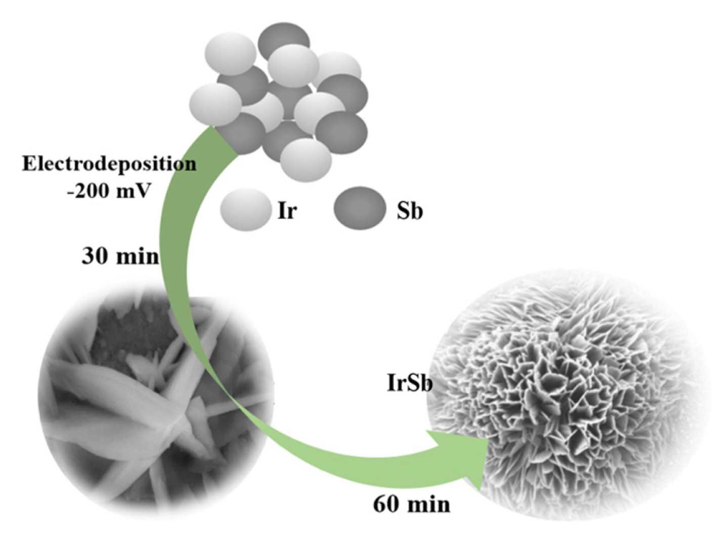
Schematic illustration of the experimental strategy to fabricate IrSb nanostructures on the electrochemically patterned.
2. Experimental
Electrochemical experiments were committed with a BAS 100B/W electrochemical workstation connected to a three electrode cell (C3 Cell Stand, BAS) at room temperature. The working electrode Au (111) is the individual crystal (111) prepared as the spherical droplets (purity 99.995%). An indium tin oxide (ITO)-coated quartz substrate with sheet resistance of 10 Ω cm−2 was used as working electrode for optical measurements. For all electrochemical experiments, the reference electrode was an Ag/AgCl (3 M NaCl) and a platinum wire was used as counter electrode. Deionized water (i.e., >18 MΩ) was used in all experiments. Ir-Sb deposition was carried out from a 0.001 M IrCl3 (Iridium(III) Chloride Hydrate, TCI), 0.001 M Sb2O3 (Antimony(III) oxide, Aldrich), and solution at pH 1.5 acidic aqueous.
Scanning electron microscopy measurements and Energy dispersive X-Ray Spectroscopy (SEM/EDS) in the analysis of were performed in ambient conditions, with a Zeiss Sigma 300 instrument. AFM imaging was performed in air using a Hitachi 5100N instrument which that can take surface topography and 3D images. X-ray diffraction patterns were acquired using a PANalytical Empyrean. Speca-Flex model XPS device was used to measure the composition of the elements, the empirical formula, the chemical state and the electronic state of the elements. To obtain information about the bonds made by atoms or molecules, WITech alpha 300R brand micro-Raman device was used. Absorption measurements were performed using a Shimadzu UV-3101 UV-vis-near-IR spectrometer at room temperature.
3. Results and Discussion
Cyclic voltammetry technique has been used to determine the deposition potentials of the electroactive Ir and Sb species in Ir-Sb solution (Fig. 1). Cyclic voltammogram of Sb taken from 1 mM Sb2O3 between −400 and 600 mV shows deposition at C1 (−100 mV) peak on ITO and Sb monoatomic layer stripping peak at A1 (200 mV), whereas A2 (20 mV) and A3 (−80 mV) shoulder peaks offset cluster stripping of Sb. C1 peak in the voltammogram of UPD area of Ir taken from 1 mM IrCl3 acidic solution between −500 and 600 mV shows approximately −350 mV cathodic peak monoatomic layer deposition of iridium.
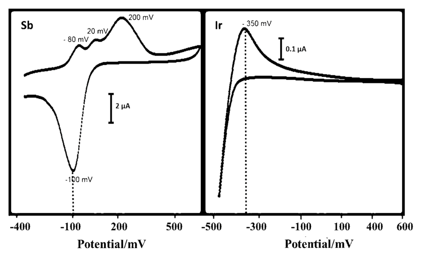
Cyclic voltamograms for the UPD regions of Ir and Sb on an Au (111) single crystal electrode at a room temperature, pH = 1.5.The scan rate was 100 mVs−1.
When the cyclic voltammogram of Ir’s UPD area taken from Au (111) electrode in an acidic medium containing IrCl3 and having a pH of 1.5 and cyclic voltammogram of UPD area of antimony taken from a medium with same pH and concentration and containing Sb2O3 is examined, as shown in Fig. 1, the area between −100 and −350 mV UPD of Ir and Sb is the deposition area for their underpotential deposition.
If the potential of working electrode is kept constant at a potential value between UPD start potential of Sb, i.e. −100 mV, and cluster deposition start of Ir, i.e. −350 mV, Ir and Sb react on the gold electrode surface and Ir-Sb film can be synthesised in well-regulated layers at an atomic level. At the same time, SEM study determined the most suitable potential as −200 mV for Ir-Sb with potential optimisation. In Fig. 2, using the SEM images of Ir-Sb obtained at −150 and −250 mV, it has been observed that nanoflower structures have been formed in different shapes but fully desired structures would be formed as a result of electrodeposition at −200 mV. Therefore, electrodeposition potential value of −200 mV has been applied in all Ir-Sb electrodeposition works on the ITO electrode.
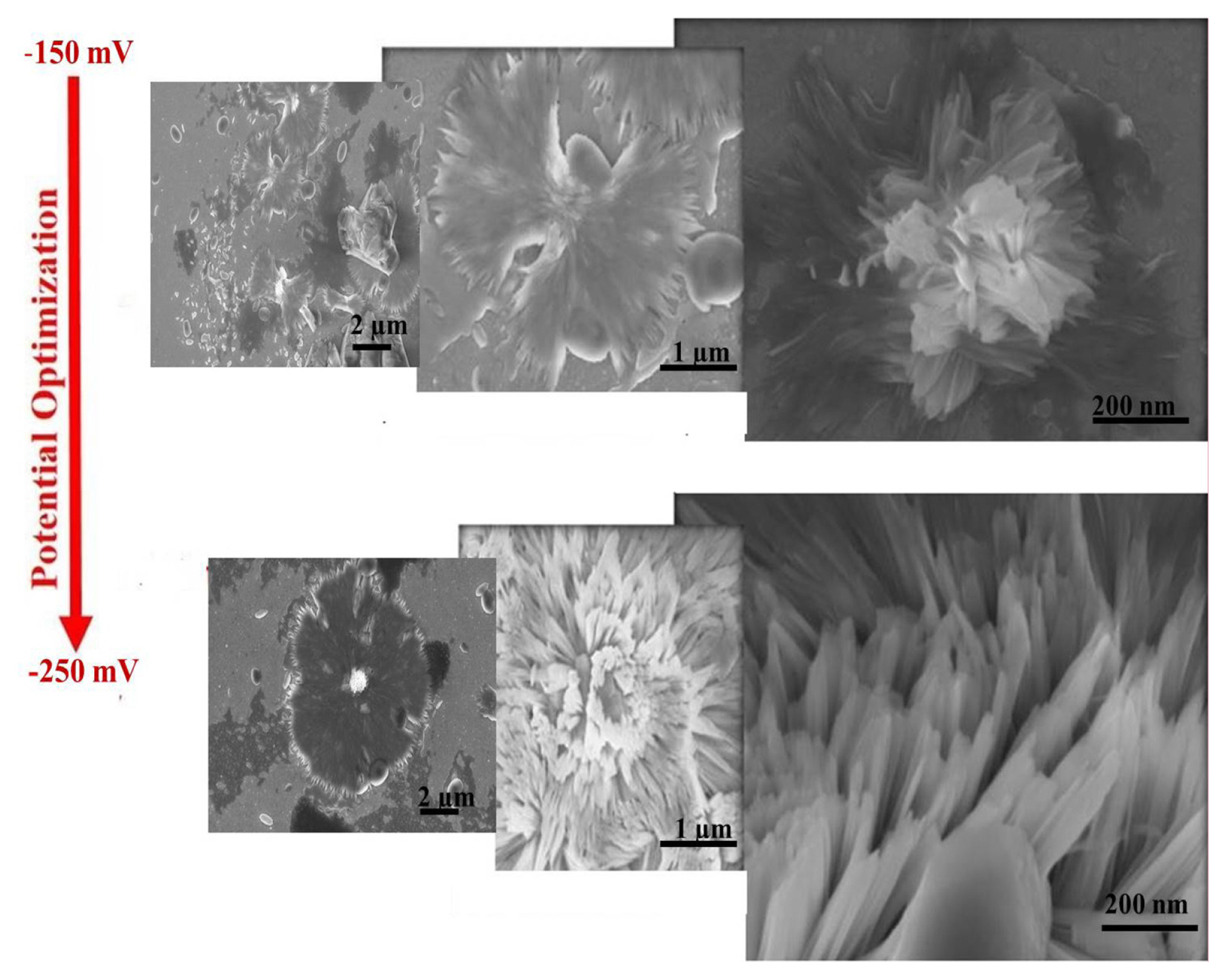
SEM micrographs of the electrodeposited for 30 minutes electrodeposition at different potentials from −50 mV to − 250 mV on ITO electrodes.
The SEM images of Ir-Sb nanostructures in different sizes and shapes, which have been electrodeposited on ITO electrodes as a result of 60 and 600 min deposition at −200 mV, are given in Fig. 3. It has been observed in the SEM images taken as a result of 60 min deposition at −200 mV that nanostructures formed in the shape of nanoflower and voids on the nanoflower structures were filled in the remaining deposition time, i.e. 600 min, and ~200 nm high nanodisk structures with high tendencies were formed by gathering and overlapping the nanoparticles (Fig. 3).
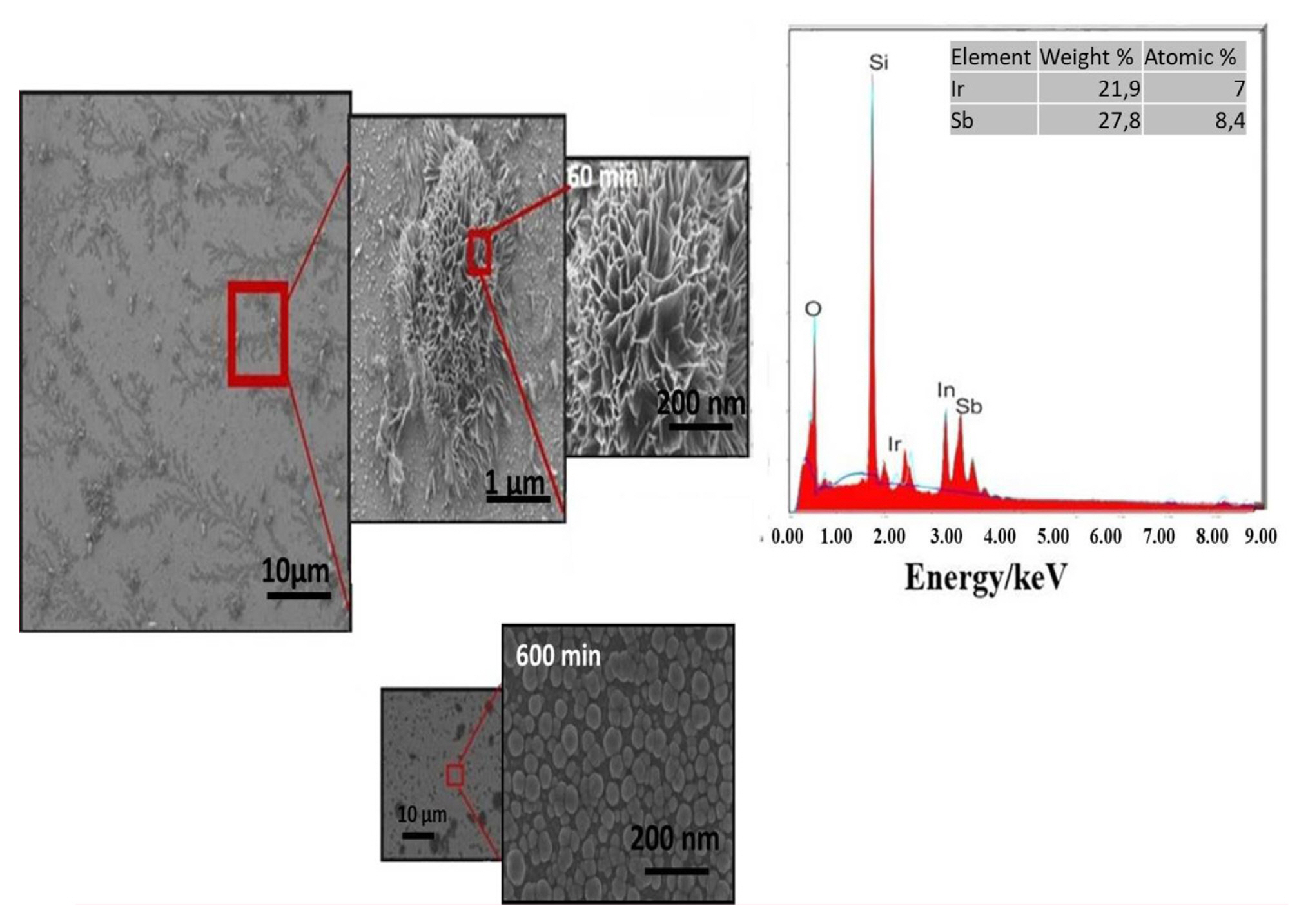
SEM images of Ir-Sb nanostructures generated as a result of potential controlled deposition of 60 min and 600 min at −200 mV on ITO electrodes and EDS spectrum of these nanostructures generated after 60 minutes deposition.
The elemental composition of Ir-Sb nanofilms has been determined using EDS technique. The EDS analysis of Ir-Sb nanofilms deposited on ITO substrates is given in Fig. 3. The qualitative and quantitative analyses of EDS spectra of films prepared in acidic aqueous solution containing Ir and Sb have shown that the structure comprises Ir and Sb, and the stoichiometry has a ratio of 1/1 (Ir/Sb). The spectra also contain indium, silicon and oxygen signal associated with ITO with the substrate under the films.
To observe the development of Ir-Sb film, 3D AFM images of Ir-Sb thin films obtained as a result of electrodeposition conducted on ITO electrodes for 60, 180 and 600 min at room temperature are given in Fig. 4. The Ir-Sb nanostructures, which have been formed by the combination of the particles gathering together with an increase in the electrodeposition duration, are arranged as fairly regular crystals. To determine the orientation of Ir-Sb crystals obtained from morphological examinations, XRD studies have been conducted. The x-ray diffractions of Ir-Sb films obtained as a result of 30, 60, 120, 240-min electro-depositions at room temperature on ITO electrodes are shown in Fig. 5. Diffraction peaks occurring at 2θ = 30.91 originate from cubic Ir-Sb (131) and other diffraction peaks from ITO substrate (ASTM, X-ray Powder Data). As can be seen, nanoflower (131) form is dominant on Ir-Sb ITO substrate. It has been observed that the intensity of the Ir-Sb (131) diffraction peak is increased with an increase in Ir-Sb film thickness depending on the electrodeposition duration.

3-dimensional AFM images of Ir-Sb nanoparticles on the ITO surface at various time (a)1, (b) 3 and (c) 5 h.
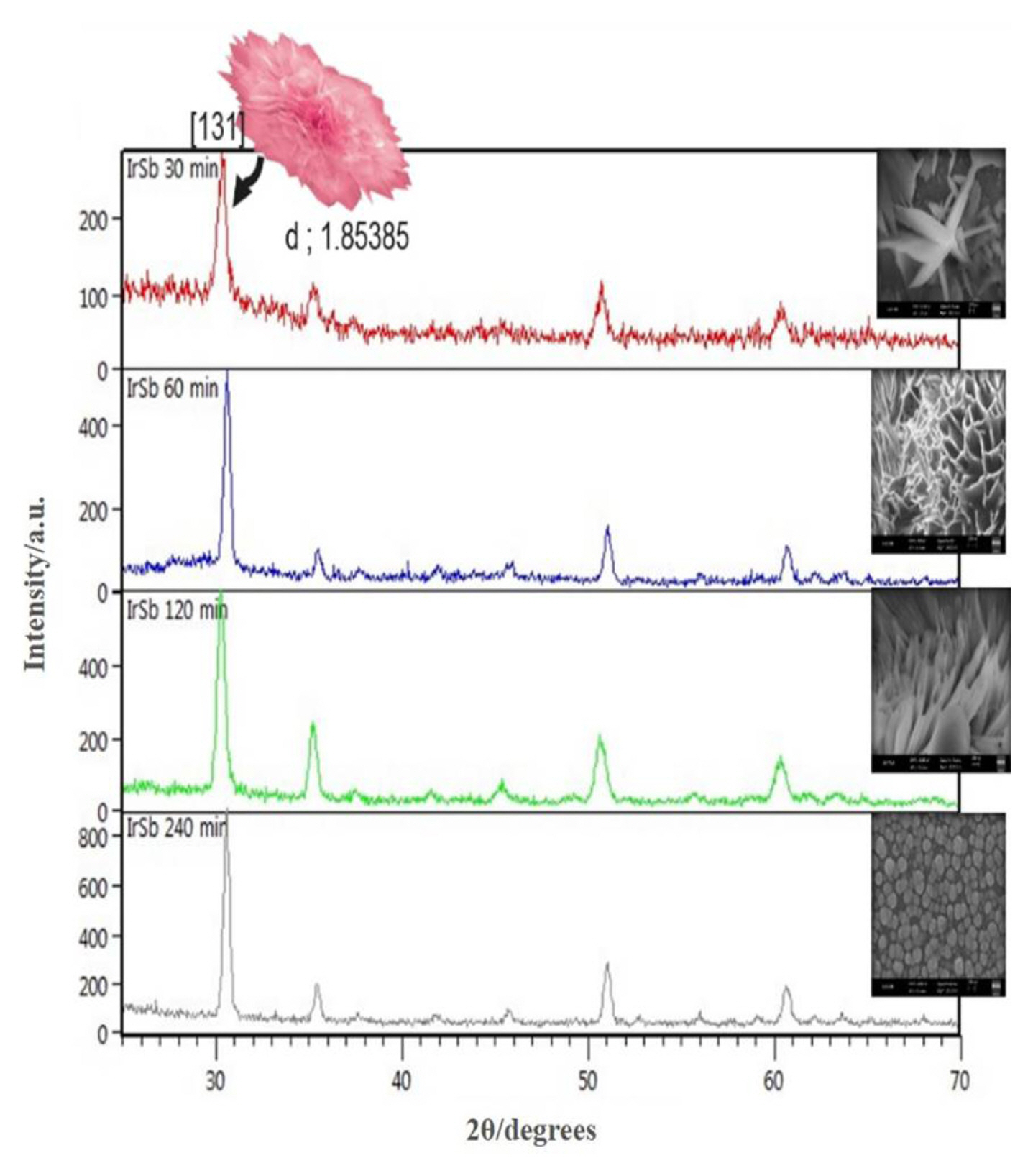
XRD patterns of the Ir-Sb thin films electrodeposited on Au(1 1 1) substrate for 30,60,120 and 240 min. Radiation source: Cu Kα.
Fig. 6 shows the Raman spectra measured by planar oriented laser polarisation of the films of Ir-Sb on the ITO electrode. The prominent main peak in the Raman spectra of the Ir-Sb generated after 60-min deposition was 406 cm−1 and the shoulder peaks were 350 and 370 cm−1 (Tolovkite), whereas the main peak of the Ir-Sb generated after 600-min deposition was 390 cm−1 and shoulder peaks were 358 and 340 cm−1 (Irarsite). These values originate from the differences among the vibrational levels of Ir-Sb modes.
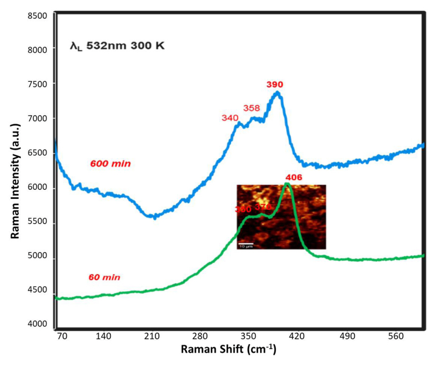
Micro-Raman spectra as measured by planar oriented laser polarization of Ir-Sb (deposition of 60 and 600 min at −200 mV) at room temperature on an ITO coated glass electrode.
XPS analysis was performed to obtain more detailed information about the species of surface components in the Ir-Sb films that have been partially analysed using EDS technique. The positions of the binding energies of Ir 4f peaks in the XPS spectra of Ir-Sb, which was electrodeposited for 60 min at −200 mV, are given in Fig. 7 as 61.0, 64 and 62.6–65.6 eV for Ir 4f7/2, Ir 4f5/2 and IrCl3, respectively. Fig. 7 clearly shows that three peaks of binding energies in XPS spectra are clearly broad and asymmetric in Sb of which 539 eV and SbO2 540 eV were obtained for 3d3/2, SbCl3.

X-ray photoelectron spectrum of Ir-Sb film grown on ITO substrate.
Fig. 8 shows the typical absorption spectrum of the Ir-Sb film synthesised on the ITO electrode using electrochemical deposition method in the 200–600 nm wavelength range. This spectrum has a shoulder absorption band corresponding to a broad electronic transition at ~300 nm. The band energy range value of the Ir-Sb films can be found using the Tauc equation. The transition process in films takes place between the valence and conductivity band and is completely related to the electronic structure of the semiconductor. The total energy and momentum of the electron-photon system are maintained during this transition process. Since Ir-Sb films have a direct forbidden energy gap, (Ahv)2’s graph against hv is linear and the point at which the ABC intersects the x-axis gives the optical forbidden energy value of the film. The point where the (Ahv)2 intersects with the x-axis, i.e. the energy axis, gives the optical forbidden energy value of the film. As shown in Figure 8, when (Ahv)2= 0, this maximum wavelength value obtained for the Ir-Sb films is ~3.8 eV, which lies in the Ir-Sb’s prohibited energy range.
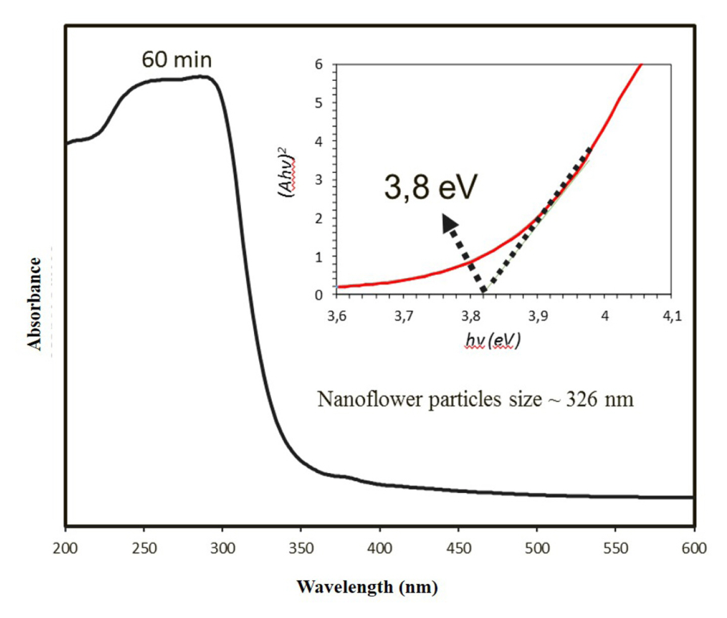
The absorption spectrum of the Ir-Sb films on the ITO coated glass electrode and the forbidden energy value found in the Tauc equation of the synthesized Ir-Sb thin film.
4. Conclusions
Herein, it has been shown that a single UPD potential deposition can be performed using the same acidic solution for the synthesis of nanoflower structures. Ir-Sb optimization has been performed that can form the basis for the alternative energy sources in the desired nanoscales by illuminating the optical and morphological structures of Ir-Sb compound semiconductor materials with nanoflower structures, which have been synthesised in a single potential by using potential-controlled electrolysis using various characterisation techniques. The AFM, SEM, Raman, XRD, XPS and UV-vis results support the superior quality of Ir-Sb nanostructures successfully synthesised by these electrochemical processes.
Acknowledgements
The financial support of this research by the Scientific Research Projects Coordinaion Unit of Ataturk University (FHD-2018-6665) is gratefully acknowledged.
Supporting Information
Supporting Information is available at https://doi.org/10.33961/jecst.2019.00073