


This paper is respectfully dedicated to the memory of late Prof. Su-Moon Park who inspired so many of us with his insights into the international nature of scientific research and the importance of collegiality and mutual respect. His work in materials electrochemistry and electroanalytical chemistry, that spanned two continents, will continue to leave an indelible mark and will undoubtedly be a source of inspiration to future generations of students.
1. Introduction
Copper (I) selenide (Cu2Se) has attracted much attention because of its optoelectronic properties and a wide range of possible applications in solar cells, gas sensors, superionic conductors, and thermoelectric converters.1-3) This material is a p-type semiconductor with a direct band gap of ~2.2 eV and is an intermediate or precursor for the preparation of the ternary compound semiconductor CuInSe2 (CIS) --- an attractive photovoltaic material because of its high absorption coefficient and stability.4,5) Thus Cu2Se has been synthesized using a wide range of methods, including hot injection,1,6) solvothermal synthesis,7) chemical vapor deposition,8) and electrodeposition.3-5)
Electrodeposition has been extensively used for the deposition of inorganic semiconductors because of its simplicity, low cost, mild conditions for film growth, and intrinsic ability to control the growth rate and composition of the film.9,10) However, this method suffers from contamination of target material with impurities (e.g., contamination of CdSe with free Se and free Cd). Given that chemical composition crucially affects the optoelectronic properties of the parent semiconductor, any candidate synthesis method must be able to control this parameter.
A simple and versatile two-step approach for the synthesis of II-VI semiconductor thin film revolves around the initial electrochemical modification of the substrate (e.g., Au) with the chalcogen (e.g., Se0), followed by its subsequent electroreduction in a chalcogen- free electrolyte dosed with suitable amount of metal ion (e.g., Cd2+). This approach was demonstrated for iron sulfide,11) cadmium selenide,12) and also for the preparation of CdSe nanoparticles in a cyclodextrin template13) and ZnTe thin films.14)
In this report, we describe a two-step approach for the synthesis of Cu2Se thin films using lactic acid; the lactate species were employed to shift the Cu2+ reduction potential via chemical complexation. Lactic acid has been extensively used as a Cu2+-complexing agent for the electrodeposition of Cu2O.22) Combined voltammetry and electrochemical quartz crystal microgravimetry (EQCM) were used to demonstrate the efficacy of the two-step approach and UV-Vis absorption spectrometry, Raman spectroscopy and photoelectrochemistry were additionally employed for the characterization of the Cu2Se thin films prepared by the two-step approach.
2. Experimental
All chemicals including copper sulfate, selenium dioxide, sodium hydroxide and sulfuric acid were from Aldrich and were used as received. Details of the electrochemical instrumentation and the EQCM set-up are given elsewhere.15,16) For voltammetry and film deposition, an EG&G Princeton Applied Research (PAR) 263A instrument equipped with Model M250/ 270 electrochemistry software was used. For EQCM, a Seiko EG&G Model QCA 917 instrument consisting of an oscillator module (QCA 917-11) and a 9 MHz AT-cut gold-coated quartz crystal (geometric area, 0.2 cm2) working electrode, a Pt counter electrode, and a Ag/AgCl/3 M NaCl reference electrode, was used. All potentials below are quoted with respect to this reference electrode. Prior to the electrodeposition experiments, the cleanliness of the gold electrode was checked by cyclic voltammetry in 0.5 M H2SO4. The potential was cycled between −0.9 V and 0.6 V until the voltammetric and frequency signals were stable.16) A tin-doped indium oxide (ITO) glass slide (12 ohm/ square) was used as a fi lm support in some experiments. The ITO electrode was sonicated in a mixture of ethanol/H2O (1:3) and acetone/H2O (1:3) for 20 min. respectively and finally rinsed with distilled water.
The electrodes were irradiated with a 300 W xenon lamp that was in a Muller Elektronik-Optik LAX 1530 lamp housing connected to a Muller Elektronik-Optik SVX 1530 power source. The light intensity measured on the electrode surface with a Newport Model 70260 radiant power meter combined with a Model 70268 probe was ~100 mW/cm2 in all the experiments described below. The exposed area of an electrode was 0.2 cm2. Absorption spectra and diffuse reflectance of the samples were measured at room temperature with a Perkin Elmer Lamda 25 UV-VIS spectrometer equipped with an integrating sphere (Labsphere RSAPE- 20). Raman spectra were measured using the 532 nm line of an Ar+ ion laser (JASCO NRS-3200) at room temperature.
3. Results and Discussion
Fig. 1 shows a combined linear sweep voltammogram and simultaneous frequency (mass) change for the Se-modified Au electrode in 1 M lactic acid solution (pH = 9). The pH of a 1M lactic acid solution was carefully adjusted to 9 with 4 M NaOH solution. The Au electrode was pre-modified with Se at −0.4 V for ~700 s in a 0.1M H2SO4 solution containing 10 mM SeO2. The peak at −0.75 V can be assigned to the reduction of Se to Se2−, which is manifest from the frequency increase (mass decrease) accompanied by the cathodic peak.12,13,17) From a comparison of frequency changes observed during the deposition and stripping steps, the electrodeposited Se was seen to be completely reduced and stripped during the negative-going scan.
Fig. 1.
Linear sweep voltammogram (solid line) and the simultaneous frequency change (dashed line) for the Semodified Au electrode in 1 M lactic acid electrolyte (pH = 9). Se was pre-electrodeposited on the Au electrode at –0.4 V for ~700 s in a 0.1 M H2SO4 solution containing 10 mM M SeO2. The inset shows a charge–mass plot during the linear scan from −0.74 to −0.84 V. Scan rate: 10 mV/s.
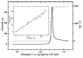
Another piece of evidence supporting the above assignment of the −0.75 V peak to Se electroreduction is presented in the inset in Fig. 1, which shows the charge-mass plot obtained during the negative-going scan from −0.76 V to −0.79 V. The range was chosen due to the substantial change of frequency. The number of electrons transferred (n) during reduction was calculated from the slope of the charge-frequency plot by combining the Sauerbrey equation and Faraday’s law:15)

In Eq. 1, Q is the charge, F the Faraday constant, k the sensitivity factor, M the molar mass, and Δf the frequency change. Thus, the n value calculated from the slope was found to be 1.9, clearly showing that the peak at −0.75 V arises from the electroreduction of Se to Se2-.
Fig. 2 contains chronoamperometric and EQCM data for a Se-modified Au electrode at a fixed potential of −0.8 V in lactate solution with and without copper ions. When the 1 M lactic acid blank electrolyte (pH = 9) contains no copper ions, the EQCM frequency increased, and mass loss due to Se reduction to Se2− was completed within ~30 s as demonstrated in Fig. 2(A). By contrast, when 10 mM copper ions were present in the 1 M lactate blank electrolyte, the frequency initially increased and then decreased signaling a net mass increase, which is consistent with formation of Cu2Se on the Au electrode surface (Fig. 2B). A simplified representation of the formation of Cu2Se on the electrode can be described below neglecting the complexation of copper with lactate:18)


Fig. 2.
(A) Current flow (solid line) and corresponding and frequency change (dashed line) for a Se-modified Au electrode at a fixed potential of −0.8 V in 1 M lactic acid (pH = 9). (B) As in (A) but with the addition of 10 mM CuSO4 to the 1 M lactic acid.
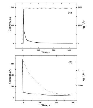
The initial increase in frequency followed by mass increase is consistent with Reactions 1a and 1b. Note also that the current is higher in Fig. 2(B) when copper ions are present than in Fig. 2(A) when no copper ions are present. This behavior supports Reaction (2), which requires more charge for the formation of Cu2Se from the reduction of Se in 1 M lactate electrolyte containing copper ions (Reaction 2), compared with the reduction of Se in blank electrolyte (Reaction 1a). The number of electrons transferred (n) during the reduction was calculated again, and was found to be ~3.9, confirming the formation of Cu2Se according to Reaction 2 in a 4e− step.
The mass was substantially increased when the same potential of −0.8 V was applied to the bare Au electrode in 1 M lactic acid containing 10 mM CuSO4, unlike the data in Fig. 2(B). This important result signals that free (metallic) copper was not substantially deposited on the Se-modified Au electrode.
To make further confirmation for the formation of Cu2Se, Raman spectroscopy was performed on the film synthesized by the procedure described in Fig. 2(B). The intense peak in Fig. 3, observed at 260 cm−1, is in good agreement with the value in previous reports for Cu2Se.19) This peak has been assigned to the Se-Se stretch vibration in Se2−.19) The absence of a peak at ~237.3 cm−1 confirms that the film contains no substantial amount of Se.20) This fact is further elaborated below.
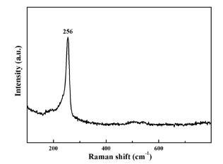
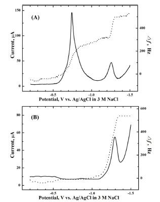
Fig. 4 shows the effect of reaction time on the composition of the film. When a potential of −0.8 V was applied for 3 s to the Se-modified Au electrode in 1 M lactic acid containing 10 mM CuSO4, the resultant film contains substantial amount of free Se as shown by the peak at −0.75 V (see above). Another peak at ~−1.3 V is due to the reduction of Cu2Se to Cu + Se2−. However, when the same potential was applied to the Se-modified Au electrode for more extended time (~60 s), the peak at −0.75 V (due to the reduction of free Se) disappeared and a peak at −1.3 V from Cu2Se reduction substantially increased. These observations and the data in Figs. 3 and 4 taken together, clearly demonstrate that the two- step approach can be successfully applied to the synthesis of Cu2Se using Semodified Au surfaces.
Fig. 4.
Linear sweep voltammograms (solid line) and the simultaneous frequency changes (dashed line) for the Cu- Se films in 1 M lactic acid electrolyte (pH = 9). Cu-Se films were prepared at −0.8 V using a Se-modified Au electrode in 1 M lactic acid including 10 mM CuSO4 for (A) 3 s and (B) 60 s. Se was pre-electrodeposited on the Au electrode at −0.4 V for ~2 kHz in a 0.1 M H2SO4 solution containing 10 mM SeO2. Scan rate: 10 mV/s.
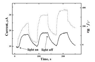
Cu2Se is a p-type semiconductor and therefore can be expected to show cathodic photocurrents upon the illumination with excitation light of suitable wavelengths.2,3) As shown in Fig. 5, the photocurrent at a fixed potential of −0.4 V in 0.1 M Na2SO4 electrolyte is cathodic, implying the film is p-type. To prevent interference, free Se was completely removed by applying −0.9 V in 1 M lactic acid blank electrolyte. Fig. 5 also presents frequency increase during photoillumination, signaling the cathodic photocorrosion of Cu2Se to Cu + Se2−. However, the lost electrode mass is regained when light is switched off in each cycle showing that the Se2− is oxidized back to Se. Similar trends were discussed in a previous report.21)
Fig. 5.
Photocurrent transients (solid line) and corresponding frequency change (dashed line) for a Cu2Se modified Au electrode in 0.1 M Na2SO4 supporting electrolyte at a fixed potential of −0.4 V. Cu2Se film was prepared by the procedure in Fig. 4(B) followed by the complete stripping of free Se at −0.9 V in 1 M lactic acid.
The UV-visible absorption spectra for Se and Cu2Se films on an ITO electrode are shown in Fig. 6. The Se film was prepared on the ITO electrode using 0.1 M H2SO4 containing 10 mM SeO2 at −0.5 V for 2,000 s while the Cu2Se film was obtained using a Se-modi-fied ITO electrode by applying −0.9 V in 1 M lactic acid containing 10 mM CuSO4. As shown in the figure, the optical absorbance increased from ~600 nm for Se and ~500 nm for Cu2Se, respectively (Fig. 6). The observed blue shift is consistent with the higher band gap energy of Cu2Se (~2.20 eV) relative to Se (~1.9 eV).2,3)
Fig. 6.
(A) Absorption spectra of Se (dashed line) and Cu2Se (solid line) film on an ITO electrode. Se was electrodeposited at −0.5 V in 0.1 M H2SO4 containing 10 mM SeO2 for 2000 s and Cu2Se film was prepared using a Se/ITO electrode by holding the potential at −0.9 V in 1 M lactic acid containing 10 mM CuSO4. (B) Diffuse reflectance data expressed in terms of the KubelkaMunk formalism for Se and Cu2Se film on the Au electrode.
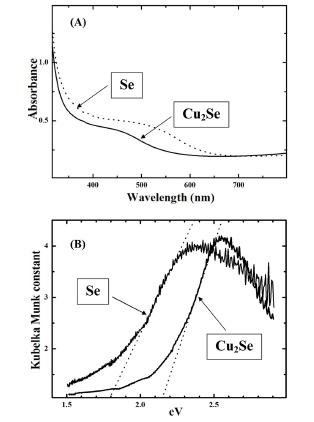
The optical band gap of Cu2Se prepared by the twostep procedure was obtained from diffuse reflectance spectra after Kubelka-Munk transformation.21) For this, a Se “precursor” film was first electrodeposited on the Au electrode at −0.4 V in 0.1 M H2SO4 containing 10 mM SeO2; the Cu2Se film was subsequently obtained by the procedure described in Fig. 2B. The band gap of electrodeposited Se was similarly obtained from the diffuse reflectance spectra. From these analyses, the band gaps of Se and Cu2Se were estimated to be ~1.79 eV and 2.15 eV, respectively in reasonable agreement with literature reports (see above).
4. Conclusions
A two-step approach for the preparation of Cu2Se thin films was demonstrated using a Se-modified Au (or ITO) “precursor” electrode surface. This pre-modified Se wa subsequently reduced (to Se2− species) in 1 M lactic acid electrolyte containing Cu2+ ions to afford Cu2Se semiconductor films.


